
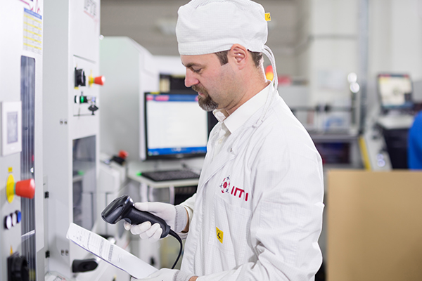
While thriving on speed and quality, we cut down time-to-market and maintain the highest product quality.
We offer rapid prototyping and make every effort to get it right the first time. By offering process development and tool design locally, you save on valuable lead-time.
Our close collaboration with you from prototyping to mass production, while our global outsourcing team procures from global competitive suppliers, ensure that you get the best quality at reasonable cost.
At IMI, New Product Introduction or NPI is a crucial process that transforms innovative concepts intro market-ready solutions – efficiently and effectively. It includes definition, development, and launch of new or upgraded devices with the goal of creating a functional prototype under ideal conditions.
Our structured NPI process enables early involvement in manufacturing, ensuring a seamless transition from development to high-volume production. This approach guarantees that products meet stringent quality standards, are manufacturable at scale, and align with customer expectations.
We actively seek meaningful partnerships with contract manufacturers early in the product lifecycle. Such collaboration accelerates time-to-market, reduces redesign costs, and enhances overall product success.
Prototyping and Manufacturing
- Quick-Turn Prototyping: Lead time of 1 week for SMT and 2 weeks for backend line.
- Standard SMT Line: Lead time of 2 weeks.
- Standard Backend Line: Lead time of 6 weeks.
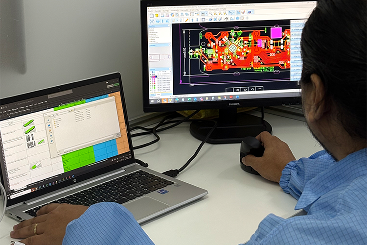
Design for Manufacturability (DFM)
- Software Tools: Vayo DFM Expert, Vayo CLM, Vayo Stencil Designer, Draftsight, LibreCAD, GC-Prevue, ViewMate Pro.
- PCB Fabrication Review: Signal layer checks, drill and route checks.
- PCB and Mechanical Assembly Review: Component spacing, SMD land pattern checks.
- Stencil Design: Solder paste printing, adhesive printing, BGA ball attach, etc.
- Panel Design: Different circuit arrangements, step-and-repeat, combo panels, multi-board designs.
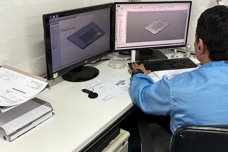
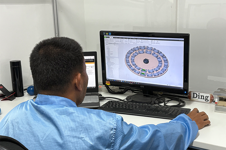
Tooling and Design Capabilities
- Tooling Design Engineers: Expertise in CAD/CAM, trim, form, singulation processes, material selection, mold design, and automation design.
- Production Jigs & Fixtures: Various holders, racks, carriers/pallets, cleaning fixtures, wire wrapping fixtures, semi-auto attachment jigs, curing jigs. soldering jigs, precision design, prototype design, sheet metal design
- Machine Design: UV curing chambers, cleaning chambers, test fixtures.
- Dimensional Drawing Generation: 2D and 3D file generation, Bill of Material (BOM) generation.
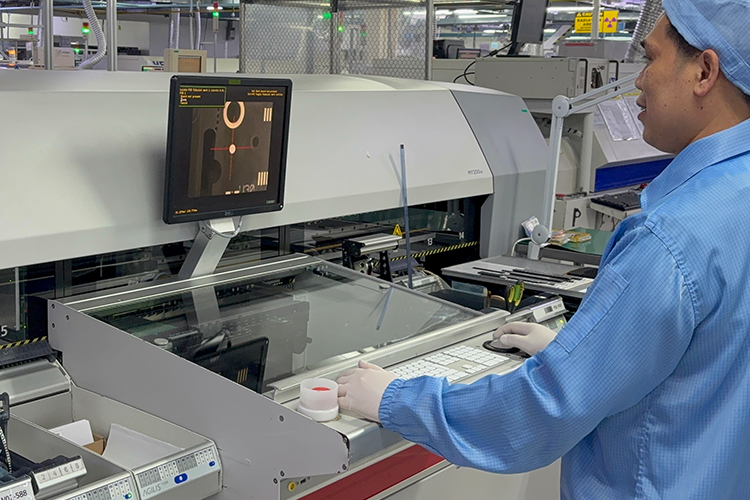
Tools and Equipment
- Jet Dispense: Stencil-free solder paste jet printing.
- Solder Paste Inspection (SPI): Automated inspection of solder paste deposit.
- Mounter: Auto Pick and Place with various capabilities.
- Reflow Oven: Flexible thermal profile.
- AOI (2D and 3D): Offline inspection with a 6-phase lighting system.
- PCBA Clean: Batch-type cleaning.
- Visual Inspection: Manual inspection with magnification.
- X-Ray: Offline oblique inspection.
- Flying Probe Tester: Various power supplies and testing equipment. No need for fixtures.