Can Our Gadgets Get Even Smaller? Yes, Thanks to EUV

The advancement of extreme ultraviolet lithography (EUV) has continued for more than two decades because it's such a challenging technology to grasp. But recently, EUV's stakeholders have managed to prepare the technology for chip fabrication in high volumes—a must in developing smaller and more powerful devices.
Computers have become essential in our daily lives, shaping how we work and live. An inevitable tech trend is computers getting increasingly compact without sacrificing memory and power, fitting the modern and mobile lifestyle. But continuous building of even smaller but high-performing chips requires breakthrough technology.
Enter extreme ultraviolet (EUV) lithography, which offers operational efficiency and supreme precision in chip printing. This allows manufacturers to put more transistors into a chip, translating to more robust processing. According to this article, high-numerical-aperture (High NA) lithography, EUV's latest evolution, will fuel the global semiconductor market by 67%, from US$600 billion to more than US$1 trillion by 2030. This is because EUV will be crucial to chip production for advanced utilizations, including artificial intelligence (AI) and self-driving vehicles.
But this advancement doesn't come cheap. Machines producing this kind of chips cost at least US$330 million. But global manufacturing giants still invest in the technology because of its innovation possibilities.
One of these is Intel, which recently announced its EUV chip production. The multinational semiconductor corporation is venturing into mass production using seven EUV machines and technology developed in its Oregon facility. Meanwhile, its Fab 34 in Ireland has begun high-volume fabrication of EUV chips, aiming to position Intel as a manufacturing leader in Europe.
What is EUV?
EUV technology is a significant catalyst for the semiconductor industry's advancement. When used for lithography—the process of printing complex patterns onto semiconductor components—EU fosters innovation because it uses shorter wavelengths of around 13.5 nanometers. This enables the more accurate printing of smaller details on chips.
How does this work? The microchip is first covered in photosensitive material, then exposed to the light, collected and controlled through optics and extremely flat mirrors. This concentrated EUV light passes through a circuit design, allowing it to be etched onto the wafer through a chemical change—a process similar to stencil art.
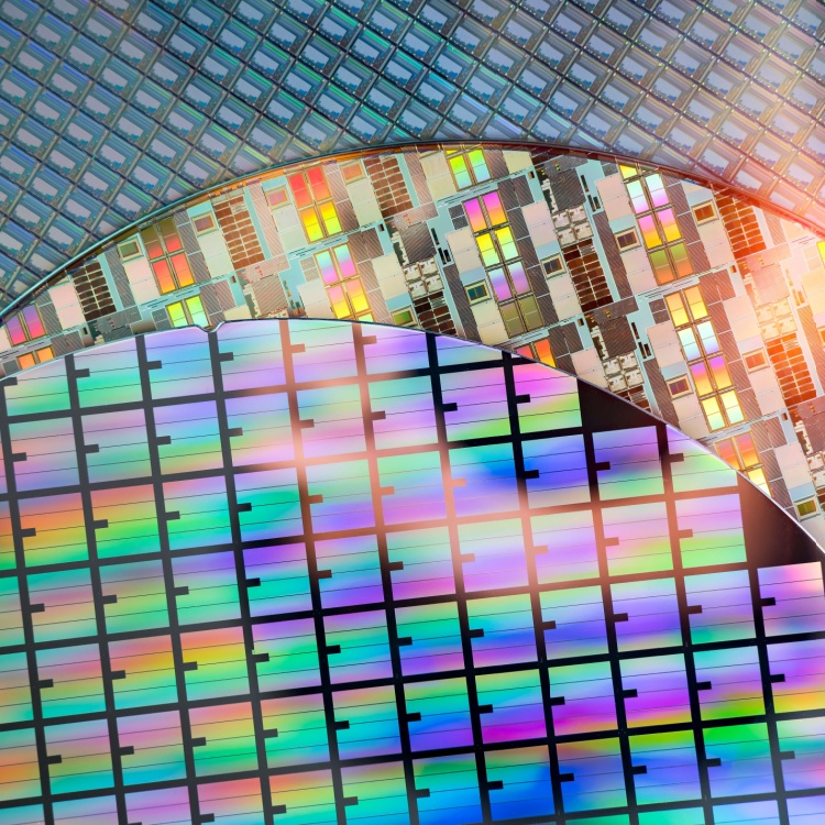
Manufacturers may place other materials in these imprinted areas to create microchip elements. Because this method can be repeated for a maximum of a hundred times with various masks, intricate circuits can be fabricated on just one wafer.
After this process, the wafer goes through additional steps to eliminate impurities, preparing the chip for slicing into individual units. These are then packaged carefully for device integration.
Deep ultraviolet (DUV) is EUV's predecessor. Compared to EUV's average wavelength of 13.5 nanometers, DUV lithography functions at at least 153 nanometers. However, DUV remains popular among manufacturers because it's already a developed technology with established training systems, infrastructure, and major funding initiatives. Also, using DUV is still ideal for bigger semiconductors used in computers, automobiles and robots.
While EUV is starting to make waves, DUV may still be standard in the coming years. This is because of its affordability and set procedures, making it more convenient. However, chip production will likely evolve soon as EUV takes on an increasingly pivotal role in the industry.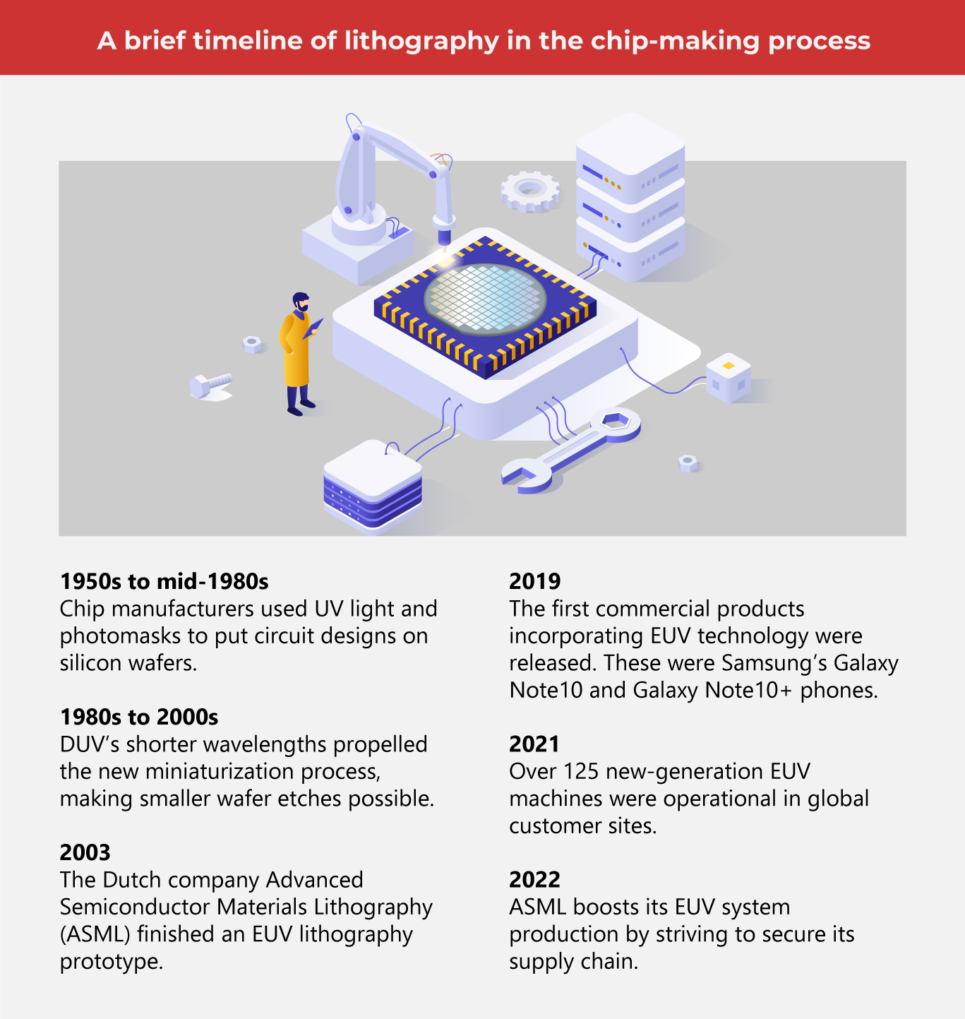
ASML, EUV tech pioneer
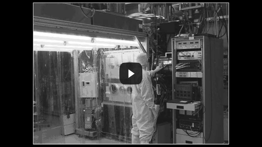
The first EUV lithography machine was released in batches and set for manufacturing from ASML. Until now, this Dutch company has been the leader in EUV development and the exclusive provider of EUV lithography systems for microchip fabrication.
Multinational tech giant IBM uses one of their most sophisticated machines—so huge that only one requires three heavy jets to convey. Made of more than 100,000 parts, the machine can print hundreds of wafers precisely and daily.
With such capable machines, the semiconductor industry can experiment with ultra-miniature circuit systems, paving the way for computer innovations.
EUV lithography, a recap
This powerful technology holds exciting possibilities, offering significant benefits for semiconductor producers. However, it's relatively new, so it still has drawbacks, which may be remedied through further research. Here's a rundown of its advantages and disadvantages.
Upsides
- Trailblazing potential
Because of its capability to produce small but high-powered chips, EUV lithography paves the way for semiconductor innovations. This can also give birth to device inventions and the flourishing of complex processes like high-performance computing systems. EUV lithography can also enable real-time data processing, which hastens AI's decision-making processes, especially useful in autonomous vehicles.
- Environmental impact
Because EUV light makes lithography more controlled and focused, the process utilizes less energy and reduces waste. EUV can also help build sustainable systems like wind farms and electric vehicles. Furthermore, scientists are looking into lowering EUV's environmental impact by recycling the hydrogen contaminated by lithography. Researchers plan to purify the hydrogen and feed it back to the machine for reuse.
- Continuous semiconductor advancement
Semiconductor technology upgrades depend on EUV lithography, which lays the foundation for compact chips that pack more power. This helps manufacturers meet their customers' ever-changing needs and develop more elaborate applications.
Downsides
- High cost
When Intel installed its EUV lithography systems this year, the company shelled out over US$150 million. Prepare to spend more for the High NA version, which may fetch over US$400 million. However, some argue that though DUV machines are more affordable, they require more labor and energy, adding to the overall cost.
- Limited supplier
As of writing, ASML is the sole manufacturer of EUV lithography systems. This challenges the semiconductor industry's growth and innovation while limiting the number of companies wanting to use this technology.
Technology is constantly shifting, and EUV lithography is a significant part of this development. Though it leaves room for improvement, researchers are working hard to boost product development so more businesses can adopt it. It's a win-win situation for everyone, including consumers looking for leveled-up gadgets.
As one of the Top 20 EMS companies in the world, IMI has over 40 years of experience in providing electronics manufacturing and technology solutions.
We are ready to support your business on a global scale.
Our proven technical expertise, worldwide reach, and vast experience in high-growth and emerging markets make us the ideal global manufacturing solutions partner.
Let's work together to build our future today.
Other Blog