Semiconductors Made Better with Lasers in 2023
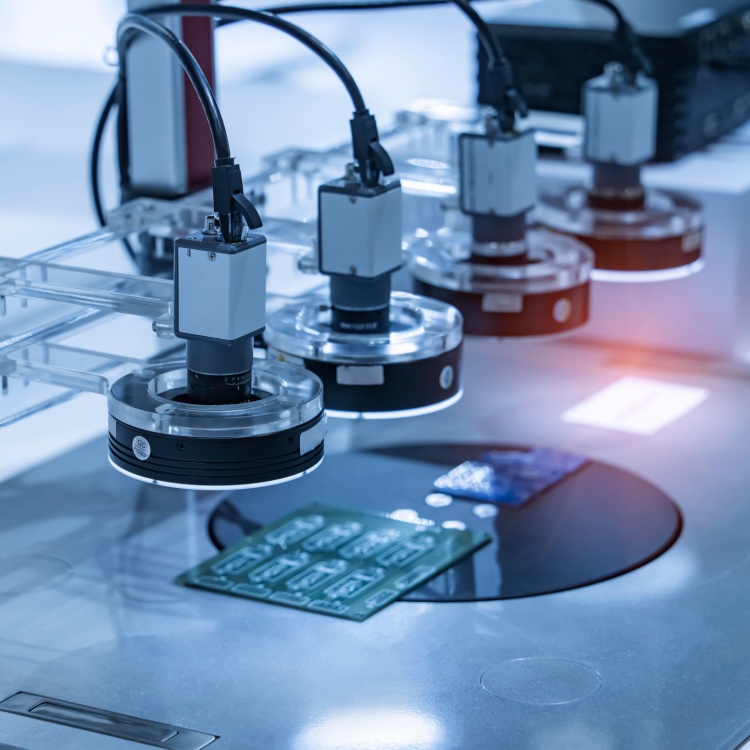
Semiconductors are vital components of a wide range of devices, facilitating the flow of electrical current between conductors and non-conductors. Consequently, semiconductor manufacturing is highly intricate, especially since gadgets are becoming increasingly compact. With this trend, smaller semiconductors need laser support and precision to do their job well.
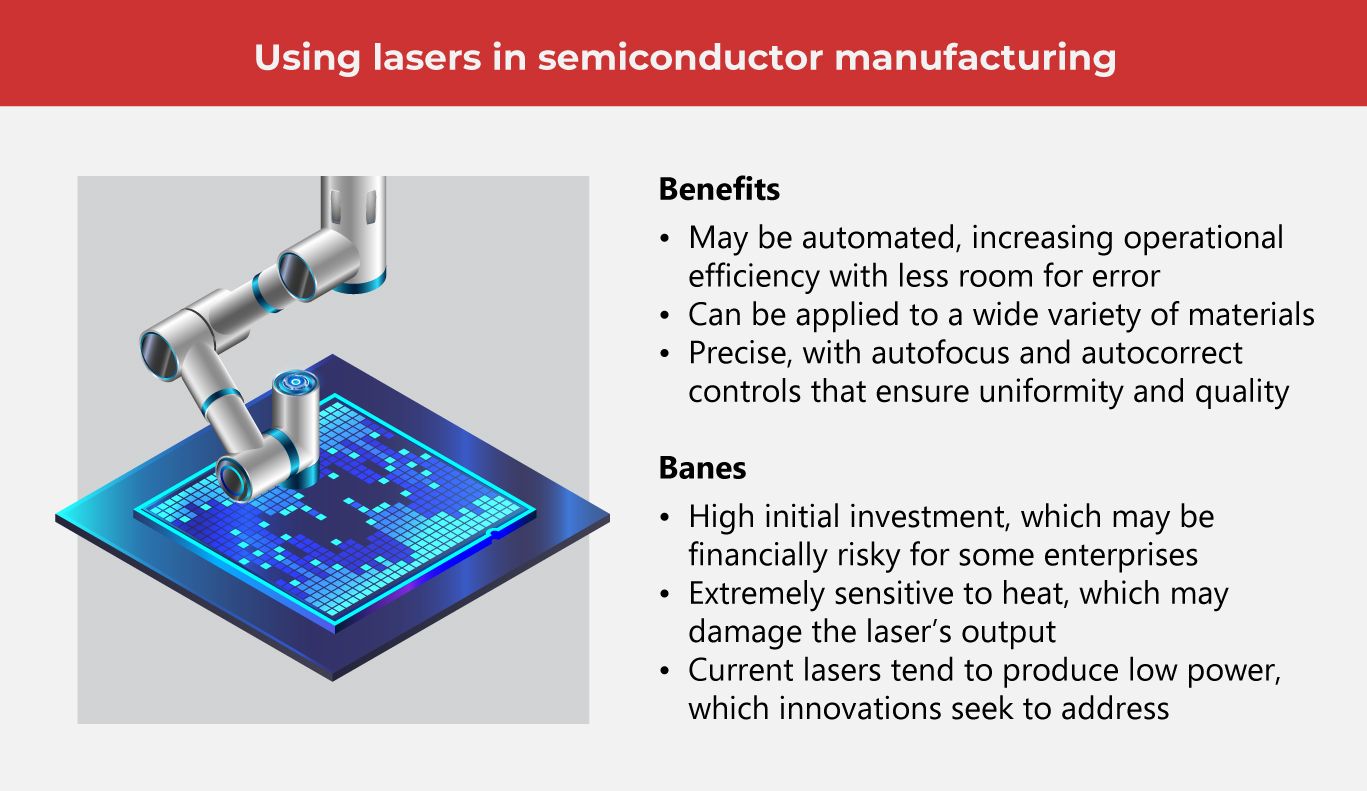
Lasers and semiconductors have been partners for decades, their alliance even more critical now in the light of fast-evolving technology. With laser applications, semiconductors are manufactured precisely, promoting better quality control. Because laser procedures are non-contact—with no tactile interaction between the tool and material—these protect sensitive components from damage and pollutants. Also, laser systems are customizable, making them adaptable to different products and processes, boosting efficiency and consistency.
Also read: SiC Semiconductors at Top Speed
What semiconductor manufacturing processes use lasers?
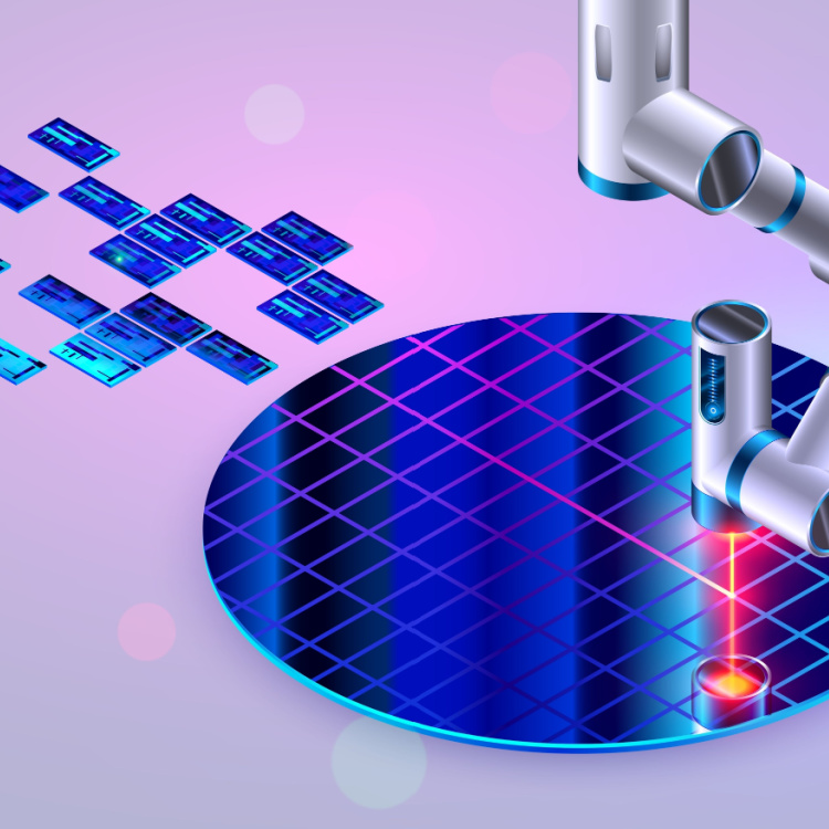
With semiconductors becoming more complex with sophisticated capabilities, laser technology lends its benefits to boost their production. Because of laser’s decreased heat impact, flexibility and high-speed processing, it is used in these semiconductor manufacturing procedures:
Cutting
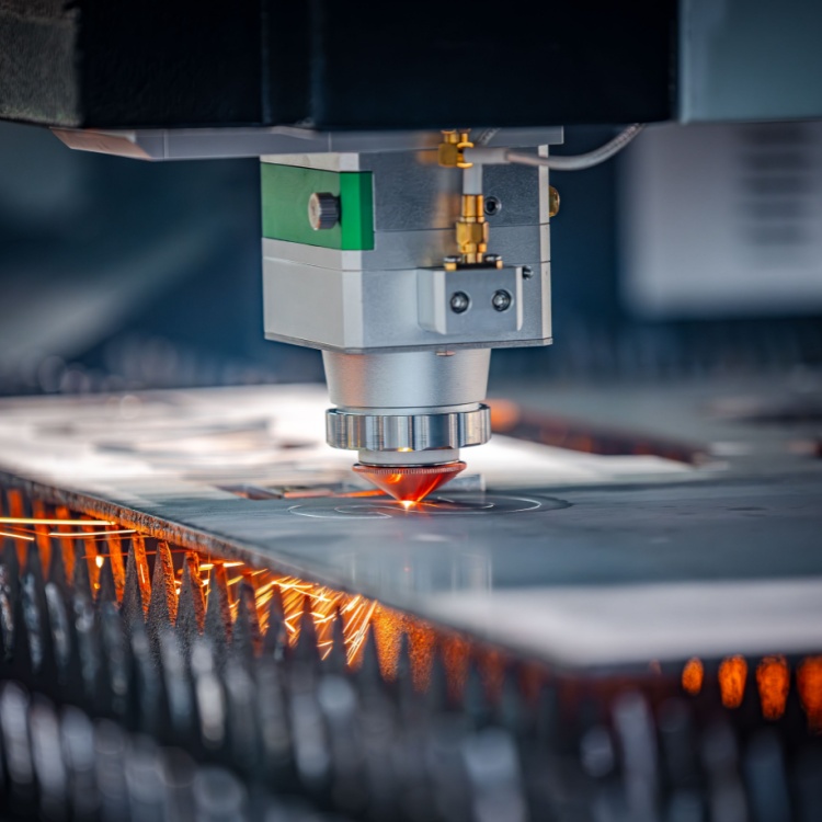
This process is essential in producing semiconductors made of wafers extracted from crystal blocks, and stencils cut out from films. With lasers that channel their robust energy into thin beams, cutting can be done cleanly and accurately. Precise cutting is necessary to install semiconductors in different devices like computers and phones properly. Other advantages of using lasers for cutting include the prevention of tool wear and material loss, which translates to higher product yield.
Scribing
Instead of cutting, semiconductor manufacturers sometimes use scribing for specific applications, like chopping up alumina substrates to make chip carriers and extracting chips from silicon wafers. Scribing involves drilling tightly spaced or intersecting holes partially through the material. Different materials require different lasers. For instance, alumina utilizes carbon dioxide lasers, while silicon is best cut with Nd:YAG (Neodymium: Yttrium-Aluminum-Garnet) lasers. Compared to cutting, scribing is much faster.
Welding
Also called laser diode welding, laser welding melts together connected sections, such as wafers and supporting plates. A laser marks the plate where adhesion will occur, then abrades its surface to ensure that the two components are joined together. After welding, the laser removes the ridges produced during abrasion—a process called deburring.
Coating removal
Lasers allow manufacturers to identify defects without taking apart the product and possibly damaging it. This is done by removing the coating, whether resin, copper, gold plating, or a thin film layer. The laser’s accuracy and narrow beam allow manufacturers to eliminate extra material while avoiding product damage.
Marking
Semiconductors are marked with lasers so they can easily be traced and read. This is especially important when monitoring production stages and during distribution, wherein defect categories are easier to spot and categorize. Marks can be very small, only readable through the microscope. While these can be etched and visible, marks can also be annealed using a process that rearranges molecules. This produces a contrast on the chip’s exterior that can only be seen when light bounces off it.
Measuring
Laser sensors are used for measuring semiconductor properties in the fabrication process. Examples of measurables are thickness, level of wear, heat, mold height, shapes, and wire length.
Top 3 laser technology trends
Despite the multiple benefits lasers currently contribute to global manufacturing, their technology is still changing and improving. Here are some of the innovations currently in the works:
- The use of epitaxial regrowth
Manufacturers use epitaxial regrowth to produce semiconductor layers with particular profiles, which are vital in device performance and integrated circuits. Now, engineering specialists are using this process to boost laser capabilities. Epitaxial regrowth for indium phosphide lasers is often used in telecom, data communication and 5G to reduce the loss of digital feedback and optics while boosting thermal extraction. Meanwhile, scientists are experimenting with gallium arsenide in lasers, boosting its performance and making it applicable in biomedical imaging, industrial manufacturing, and silicon photonics.
- High-brightness lasers
Kyoto University researchers aim to produce even brighter lasers by altering the composition of PCSELs or photonic-crystal surface-emitting lasers. Brightness is a good indicator of the laser’s level of focus, ensuring that its beam doesn’t deviate. To make PCSELs applicable in large-scale operations, researchers utilized photonic crystals implanted in the laser with an adjusted internet reflector, allowing oscillation on a broader area. This technique addresses heat disruption, allowing the laser to retain its bright beam continuously.
Through experimentation, scientists developed a PCSEL spanning 3 mm, a considerable improvement from the former one mm-diameter. The study’s next aim is to create a laser diameter of 10 mm, which generates a kilowatt of power. The Japan-based group also uses nano-imprint lithography to manufacture the photonic crystal, which operates in faster speeds compared to electron-beam lithography.
- Compact laser technology
Most of today’s lasers are produced from stiff and fragile semiconductor crystals. But researchers at the University of St. Andrews in Scotland are experimenting with organic semiconductors, which are flexible, carbon-based, and capable of producing visible light. Though these are already used in OLED (organic light-emitting diode) phone screens, a downside of organic semiconductor lasers is that they usually require another laser to fire them up.
But St. Andrews scientists have developed an organic semiconductor laser powered by electricity to remedy this. The team first fabricated an OLED with a massive light yield fused with a polymer laser structure. The result is a novel type of laser that produces a green beam of brief light pulses. Aside from using less manufacturing energy, this breakthrough may facilitate communication between OLED displays and has potential applications in detecting disease, spectroscopy, and pinpointing environmental hazards.
Laser development has become crucial, especially with today’s rapidly advancing electronic devices. The benefits of boosted laser technology, including precision, flexibility, efficiency and quality, all contribute to semiconductor development, which produces high-performance gadgets and machines that lighten the burden of humanity’s endeavors.
As one of the Top 20 EMS companies in the world, IMI has over 40 years of experience in providing electronics manufacturing and technology solutions.
We are ready to support your business on a global scale.
Our proven technical expertise, worldwide reach, and vast experience in high-growth and emerging markets make us the ideal global manufacturing solutions partner.
Let's work together to build our future today.
Other Blog