The Role of SiC Wafers in Power Semiconductor Manufacturing
Key Takeaways
- SiC wafers are becoming increasingly important as demand grows for high-performance power electronics.
- Silicon carbide offers material properties suited to high-voltage, high-temperature and high-frequency applications.
- Wafer quality can influence downstream device performance, reliability, and manufacturing yield.
- Moving from 150 mm to 200 mm wafers could improve production economics, but larger substrates also introduce new process-control challenges.
- Defect control, surface quality and epitaxial uniformity remain important considerations in SiC wafer production.
- Electric vehicles, renewable energy, industrial equipment, and charging infrastructure are among the key application areas for SiC power devices.
- Scaling SiC successfully will require progress across crystal growth, wafer processing, epitaxy, inspection, and device manufacturing.
Power electronics is being asked to deliver more power from smaller, more efficient systems. Electric vehicles need compact power conversion. Renewable energy infrastructure has to handle changing electrical loads. Industrial equipment increasingly operates under demanding thermal and electrical conditions.
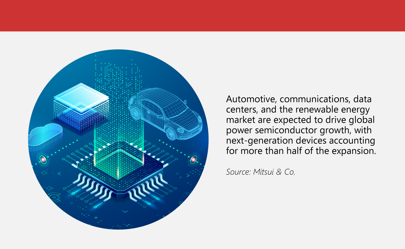
These requirements are contributing to greater interest in SiC wafers and the devices produced from them. Silicon carbide offers properties that make it attractive for demanding power applications, but the material potential depends heavily on how consistently it can be produced and processed.
Why Silicon Carbide Is Getting More Attention
Silicon remains the dominant semiconductor material across much of the electronics industry. Its manufacturing ecosystem is mature, extensive, and cost-efficient.
SiC offers a different set of properties for power electronics applications. It has a wide bandgap, high breakdown field, and high thermal properties which are suitable for high voltage, high temperature, and high switching frequency applications.
That makes SiC particularly relevant to power devices such as MOSFETs and diodes.
The benefits can be greater than the sum of its parts. Switching speeds and losses may affect cooling, passive component sizes and overall design of a power-conversion system.
A SiC Wafer Has a Long Manufacturing Journey
A finished wafer is the result of several tightly controlled manufacturing stages.
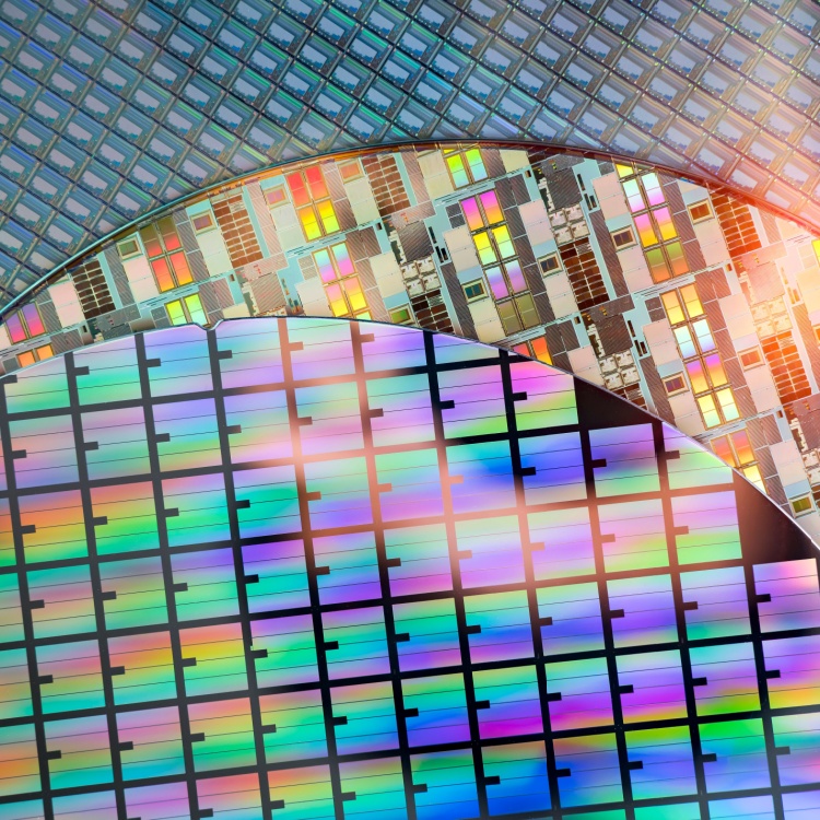
The process begins with crystal growth to produce a SiC boule. That material is then sliced, ground and polished before further processing. Depending on the application, an epitaxial layer may subsequently be deposited on the substrate.
This is one reason SiC wafer manufacturing presents a different challenge from simply producing a larger piece of semiconductor material.
Where Wafer Quality Can Make a Difference
Defect control is one of the less visible but important aspects of SiC manufacturing.
Crystal-growth imperfections, surface defects and variations in material properties can affect downstream processing. Manufacturers therefore need inspection and characterisation methods that can identify problems across the wafer.
Fraunhofer IISB, for instance, describes techniques including X-ray topography, optical inspection and photoluminescence mapping for analysing SiC substrates and epitaxial layers. These methods can help connect material characteristics with device performance and reliability. (iisb.fraunhofer.de)
The larger point is simple: a wafer should not be assessed only by its appearance or basic specifications. Its characteristics need to support the processes that follow.
Bigger Wafers Could Change Production Economics
Wafer diameter has become an important part of the SiC manufacturing conversation.
Larger substrates place greater demands on crystal growth, slicing, polishing, epitaxy, metrology, and process control. Small variations that might be manageable on one part of a smaller wafer can become more consequential when manufacturing across a larger surface.
The transition therefore requires more than new equipment. It requires consistent control across the entire process.
These considerations extend beyond wafer production into downstream device fabrication and power module manufacturing, where material consistency can influence subsequent assembly and reliability requirements.
Which Industries Are Driving SiC Demand?
SiC’s best applications usually involve cases with high expectations regarding parameters like power density, switching performance, voltage capability, and thermal management.
For instance, electric vehicles are an excellent example. Types of SiC devices are used for a traction inverter in the conversion of high power.
However, SiC is not considered the best material for every design. In many instances, the use of silicon is economically viable and effective.
The choice of material for the system depends on its specification and costs.
What SiC Means for the Broader Electronics Supply Chain
The development of SiC power semiconductors is not happening in isolation. Better substrates and more scalable wafer processes support the device manufacturers and power semiconductor packaging operations working downstream. Once fabricated, SiC dies must be packaged in ways that manage electrical, thermal and mechanical demands before they can be integrated into larger power systems.
This creates a direct connection between semiconductor material quality and the reliability of the systems that eventually use it.
For an electronics manufacturing organisation such as IMI, understanding that connection is important. Its work across automotive, industrial and power-electronics applications places semiconductor technologies within the context of the larger systems they ultimately support. Its capabilities also extend into power module assembly services, helping connect semiconductor technologies with the packaging, testing and integration requirements of finished power modules.
With the growing popularity of SiC use, repeatability will be a bigger focus in the coming years than material performance. The issue is no longer one of whether silicon carbide can be produced to meet the necessary electrical properties. It is whether those characteristics can be manufactured regularly, cheaply and in quantities sufficient for today's electronic markets.
Frequently Asked Questions
What are SiC wafers used for?
SiC wafers are used as substrates for manufacturing silicon carbide semiconductor devices, including power diodes and MOSFETs. These devices are used in applications such as electric vehicles, renewable energy systems, industrial equipment, and charging infrastructure.
Why are SiC wafers important for power semiconductors?
SiC wafers provide the material foundation for devices designed to operate under demanding voltage, temperature, and switching conditions. Wafer quality can also affect downstream processing, device performance, and manufacturing yield.
What is SiC wafer manufacturing?
SiC wafer manufacturing involves processes such as crystal growth, slicing, grinding, and polishing. Additional steps, including epitaxial growth and wafer inspection, may be required before the material is ready for semiconductor device fabrication.
Why is the industry moving toward 200 mm SiC wafers?
Larger wafers provide more usable surface area, potentially allowing more devices to be produced from each wafer. However, manufacturers must maintain material uniformity, defect control, and process yield across the larger substrate.
Where are SiC power semiconductors used?
SiC devices are used in applications including electric-vehicle powertrains, EV charging systems, renewable energy equipment, industrial motor drives and other high-power conversion systems where their material properties can provide system-level advantages.
 As one of the Top 30 EMS companies in the world, IMI has over 40 years of experience in providing electronics manufacturing and technology solutions.
We are ready to support your business on a global scale.
Our proven technical expertise, worldwide reach, and vast experience in high-growth and emerging markets make us the ideal global manufacturing solutions partner.
Let's work together to build our future today.
Other Blog