Additive Manufacturing Gets a Boost This 2025
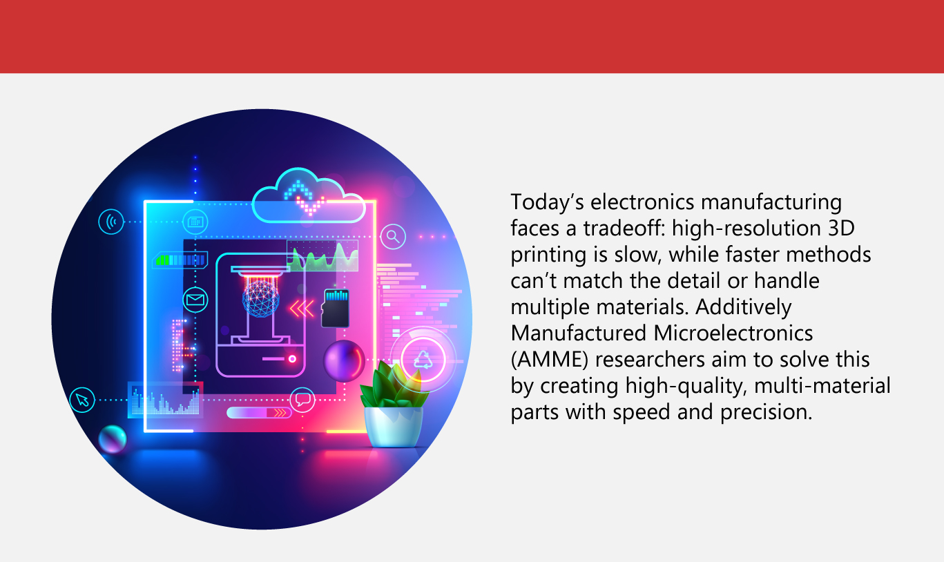
As electronics shrink and become more complex, excelling in thermal cycling tests and supporting high-frequency signals like 6G become critical. These advances demand smoother substrates and better materials. Additive Manufactured Electronics (AME) offers a promising solution, leveraging 3D design freedom to meet next-gen performance demands.
Wire bonding has been used for decades by industrial manufacturing to connect tiny circuits on a chip to larger ones on a circuit board. It works by attaching both ends of a thin wire, about the width of a human hair. Because these wires are so delicate, they’re covered in protective material and connected to a metal frame with pins or pads that link to the board. This process takes up much more space—around 10 times the size of the chip—and has to be done repeatedly since most electronics have many chips.
One of the most effective ways to improve how chips are packaged might be to skip the traditional design for manufacturing entirely. Instead, the chip could be placed directly onto the board it connects to. This method can shrink the space needed by up to 80%, making devices smaller and lighter while cutting down on materials and manufacturing costs. However, this requires a new way of connecting the chip to the board.
Additive manufacturing could solve this by printing circuits directly onto 3D surfaces. This future-ready method removes the need for bulky packaging and wire bonding, allowing smaller, simpler, and more efficient chip integration.
(Also read: Flip Chip Tech Is Here to Stay)
The evolution of additive manufacturing
Additive Manufacturing (3D printing) began in the 1980s with tool technologies like stereolithography (SLA), which built objects layer by layer from digital designs. Later methods, such as Selective Laser Sintering (SLS), Fused Deposition Modeling (FDM), and inkjet printing expanded materials and applications.
In the 1990s, new "Direct Write" methods emerged, letting manufacturers print electronic parts like circuits and antennas directly onto surfaces without traditional steps like masking. DARPA's Mesoscopic Integrated Conformal Electronics (MICE) program helped push this forward in 1999.
As 3D printing improved in the 2000s, it merged with Direct Write, creating 3D Printed Electronics—fully functional electronics built into 3D objects. This opened up new uses in areas like aerospace and healthcare. To support this growing field, IPC later set standards for Additive Manufactured Electronics (AME), which combines both technologies to create smarter, lighter, and more flexible devices.
 (Also read: It’s a Bold New 3D Printed World)
Emerging methods in AME
As AME evolves, several innovative approaches are being explored to improve operational efficiency.
-
Direct Digital Manufacturing (DDM)
Conventional methods in manufacturing industries often need expensive molds and tooling, making production slow and costly. DDM removes this by using digital processes, allowing faster and cheaper prototyping.
The nScrypt system, designed for Direct Digital Manufacturing (DDM), integrates various tools such as fused filament fabrication (FFF) 3D printing, milling, micro-dispensing, and pick-and-place capabilities. These components operate in coordination through instructions provided by a CAD file.
Additionally, this system uses different tool heads for various materials and processes, enabling the creation of complex circuits. DDM and AME follow unique design rules that differ from traditional printed circuit board (PCB) methods, streamlining fabrication and offering production flexibility.
-
Fused Filament Fabrication (FFF)
Through FFF, melted thermoplastic is extruded through a nozzle, creating low-cost and precise parts. To refine the surfaces, milling is used to smooth and flatten the FFF substrates.
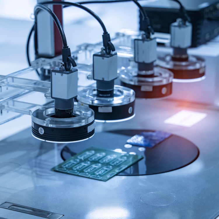
Components are then placed using a pick-and-place method, with a vacuum nozzle and camera to ensure accurate positioning.
The chip contains short pairs of pads, allowing the quality of the connections to be checked by measuring resistance and continuity between them. This process ensures that interconnects function properly, boosting product design and development.
-
Printing on glass substrates
This method 3D prints small circuits directly onto glass using silver as the conductive material. Instead of a traditional filament, silver paste is applied using micro-dispensing, ensuring precise placement.
The silver particles, just 35-50 nanometers in size, form strong electrical connections when heated to 250°C. After dispensing the paste, a Quad Flat No-lead (QFN) chip is placed on the glass using a pick-and-place process. The glass substrate is stable, smooth, and non-conductive, making it ideal for precise electronics.
This technique promotes miniaturization, producing high-performance circuits without plastic materials, suitable for applications requiring durability and heat management.
The AME method has successfully created compact, high-functioning circuits on plastic and glass surfaces. This shows AME's strong potential to support future electronics that need to be small, powerful, and adaptable. Looking ahead, researchers may focus on material composition analysis, improving material conductivity, and fine-tuning fabrication steps to improve device quality and unlock new possibilities in cutting-edge tech applications.
Top 5 benefits of AME
AME is reshaping the design and engineering of electronic devices, offering new possibilities that go beyond what traditional methods allow.
-
Speedy prototype building
AME makes it easier and faster to build and test small, complex parts like sensors and antennas right on-site. Unlike older methods that are slow and costly, AME boosts engineering capabilities and supports quick changes.
-
Design freedom
AME allows complex shapes and built-in electronics in manufacturing. It lets them 3D-print both wiring and insulating parts simultaneously, making it possible to create smaller, smarter devices. This reduces the need for extra assembly and helps keep electrical signals clean and strong.
-
Cost-efficient circuit boards
AME makes it possible to 3D-print working circuit boards quickly and affordably. Instead of waiting on outside manufacturers, teams can test ideas faster, tweak designs instantly, and produce multiple versions. This reduces delays and cuts costs in global manufacturing, helping bring new products to market in less time.
-
Nearshoring
Relying heavily on overseas suppliers, especially in China, can disrupt production when crises hit. AME helps fix that by letting companies make parts locally, on demand, using digital files. It means fewer delays, less risk, and more control—especially useful when global supply chains are uncertain.
-
Improved functionality
AME improves functionality by using high-performance materials tailored for specific tasks, like heat-resistant substrates or low-loss dielectrics for better signal clarity. This targeted material use, combined with precise manufacturing, allows electronics to work more efficiently in harsh environments or high-frequency applications.
As AME technology continues to grow, it’s essential to build expertise and market trust. Collaborating with universities, research institutes, and organizations like IPC, the goal is to create reliable standards for 3D-printed electronics. With ongoing research and innovation, there’s hope that AME will soon transform industries, offering new possibilities for efficient, high-performance electronics worldwide. As one of the Top 20 EMS companies in the world, IMI has over 40 years of experience in providing electronics manufacturing and technology solutions.
We are ready to support your business on a global scale.
Our proven technical expertise, worldwide reach, and vast experience in high-growth and emerging markets make us the ideal global manufacturing solutions partner.
Let's work together to build our future today.
Other Blog