What’s the Last Great Step before Chips Go to Market?
The global semiconductor packaging market is set to reach $60.44 billion by 2030, according to an Opportunities and Forecast report for 2021-2023 by Allied Market Research.
It is a rapidly growing industry, growing at a CAGR of 9.10%. As our demand for more consumer electronics, electric vehicles, and technologies such as AI and cloud computing increase, so does our reliance on semiconductors. As industries attempt to keep up with an ongoing global chip shortage, engineers and technologists seek to find ways to improve and innovate how semiconductors are made.
Though the goalposts keep moving, the objective has always been to create reliable, high-performing, energy-efficient, durable, and affordable semiconductor chips.
The challenge for chipmakers today is coming up with semiconductor chips that are not only reliable, high-performing, energy-efficient, durable, and affordable, they have to smaller and more powerful, too.
Semiconductor chips are needed to power the tiniest gadget to the largest data center, so it’s no wonder that the growth opportunities for the semiconductor packaging market are tremendous.
The last step before the chips hit the market
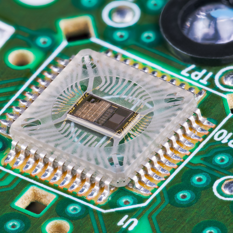
Semiconductor packaging involves wrapping or encasing the chips so these can be attached to a circuit board. Packaging protects the chip from external elements such as changes in temperature and humidity, as well as protecting the chips from pressure and impact.
Packaging ensures that these elements will not interfere with the delicate wires inside the chip. Packaging is also the process that allows the chip to communicate with other chips from within the circuit it’s a part of, as well as with other chips outside of the device it’s in.
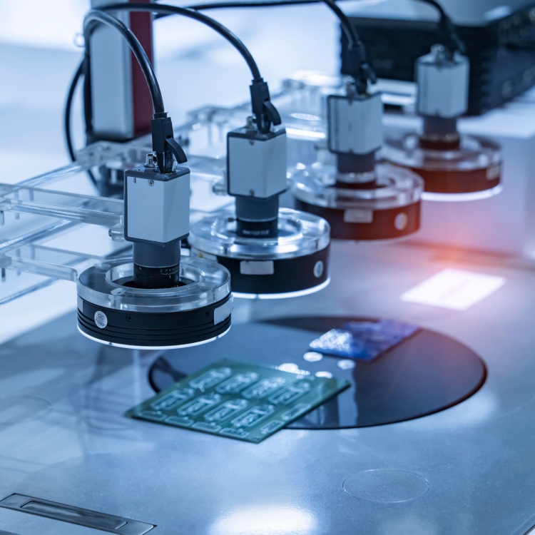
Several essential steps are involved in creating semiconductor chips, and packaging is the final step. Within this last crucial step are many processes, but there are essentially four stages to semiconductor packaging.
(Also Read: The Chip Crunch: How It Affects Automakers)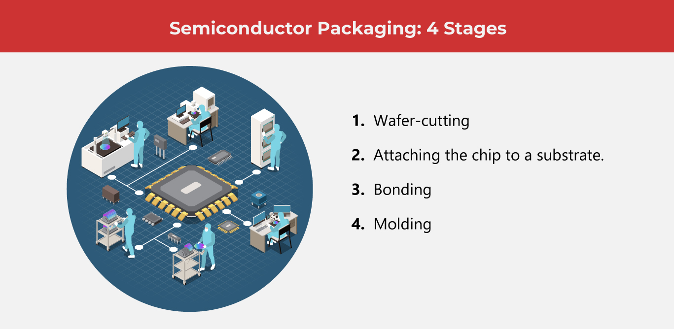
First, a semiconductor wafer is cut or sawed into smaller chips. This can be done by literally sawing the wafer or through methods such as laser-cutting.
When the cutting is done, the smaller chips are then attached to a substrate, which provides structure and support for the chips. These can be lead frames, but these can also be printed circuit boards. The substrate protects the chips and allows them to transmit electric signals between themselves throughout the circuit.
Electricity flow is achieved with the next stage, called bonding. This process connects the chip to the substrate the chip is attached to. Wire bonding is one conventional way to do this. Another is the “flip chip” method.
The difference between the two methods is that in wire bonding, the active surface of the chip is connected to the wire, with the surface facing upwards. In the “flip chip” method, it’s the surface facing downward, attached to the board, that is active.
The last stage is the molding process, which shapes the chip into the shape the manufacturer desires. It entails a process that entails sealing the chip into a chemical resin.
New Approaches to New Demands
Cherie Sasan, Integrated Microelectronics Inc.’s Head of Design and Development understands the growing market for semiconductor packaging and recommends several approaches to innovation that can propel IMI forward and allow the company to stay ahead of market demands.
First, upgrading design and development capabilities is a must, especially when it comes to computer-aided engineering (CAE) tools. The right advanced tools help advance adaptability in more complex designs. These tools reduce design time, as well as reduce, if not eliminate the need for physical prototypes.
One good example of such an upgrade would be the use of digital twinning, allowing for a working virtual double of the prototype without the need to produce it physically before it is ready to be produced at scale.
The next approach Ms. Sasan recommends is to allocate proper resources for research and development efforts and to explore new materials, technologies, and processes. These might address current global challenges related to the chip shortage. Resourcefulness almost always leads to innovation.
The third approach is investing in new process technologies, especially in the prototype assembly line. She mentions that design verification capabilities enable early detection of flaws, mitigating costs related to do-overs and prototype iterations.
These capabilities and approaches empower packaging designs that are manufacturable and testable in more efficient ways, ensuring reliability and high performance.
As one of the Top 20 EMS companies in the world, IMI has over 40 years of experience in providing electronics manufacturing and technology solutions.
We are ready to support your business on a global scale.
Our proven technical expertise, worldwide reach, and vast experience in high-growth and emerging markets make us the ideal global manufacturing solutions partner.
Let's work together to build our future today.
Other Blog