
When Quality and Reliability are Put to the Test
Can your product ace the test for quality and reliability? Find out how cutting-edge technology can ensure you bring the best, safest, and most cost-effective version of your product to market
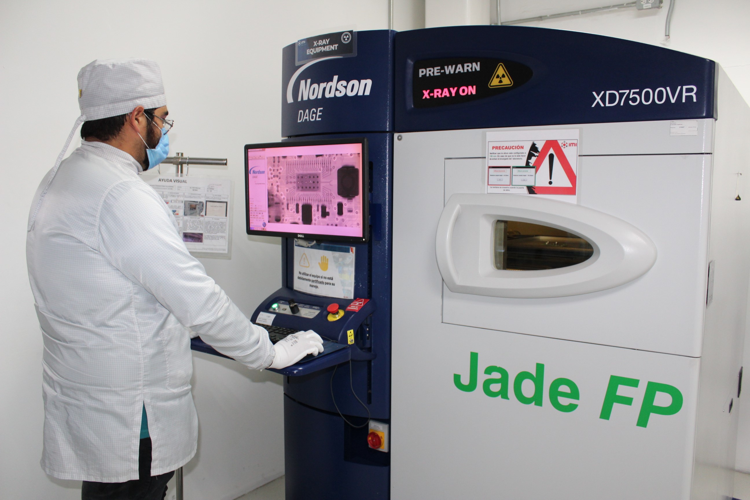
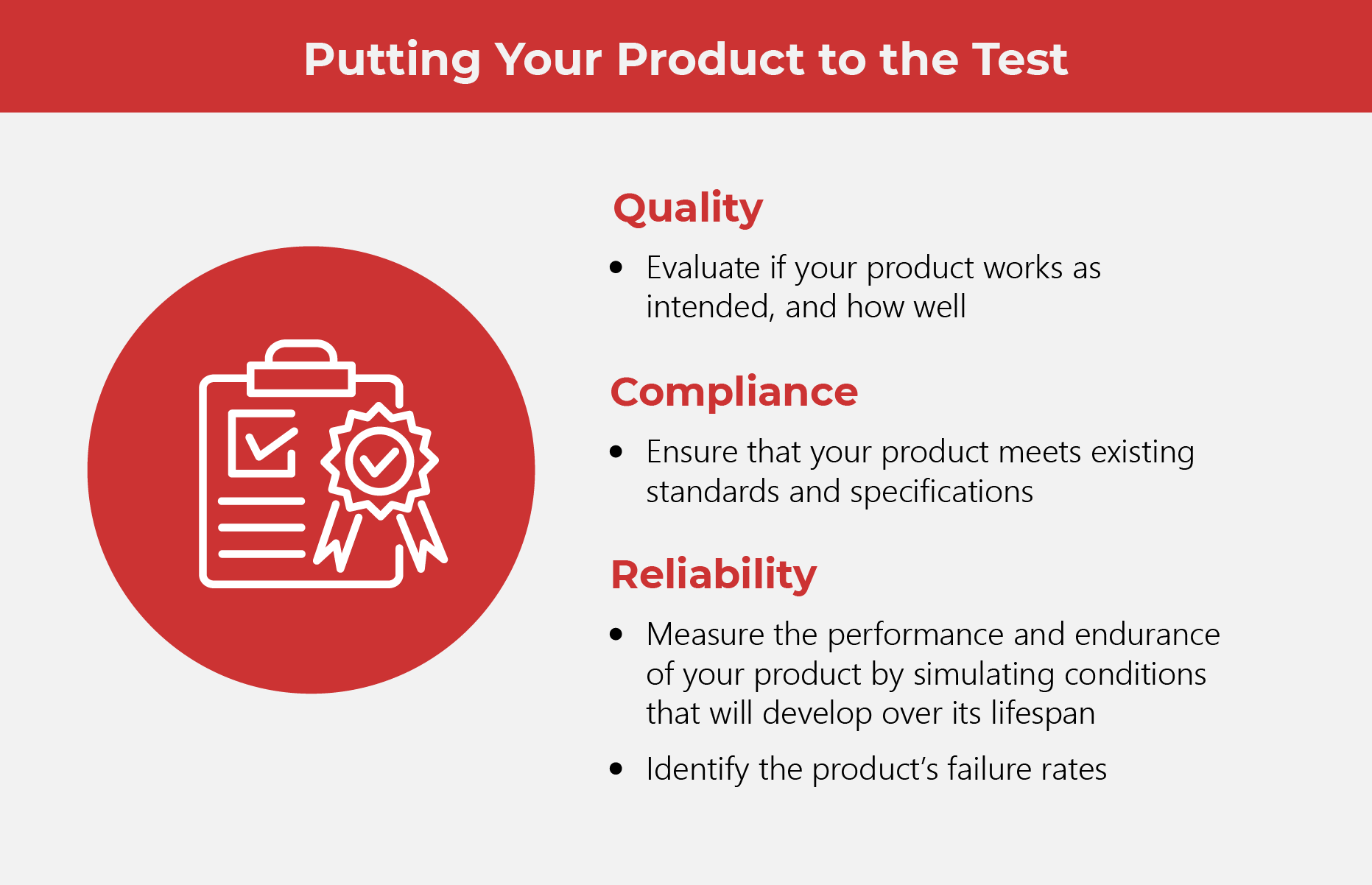
A defective product jeopardizes your bottom line, damages your brand’s reputation, and most importantly, could put your customers in danger. Before your product goes to market, precise and rigorous reliability testing and failure analysis are crucial for your business. It enables you to get the best, safest, and most cost-effective version of your product to your customers.
Tried, tested, and trusted
From life-saving medical equipment to vehicles to must-have consumer electronics, products from a wide range of industries are tested for quality and reliability. This ensures the product meets regulatory requirements and functions properly. It evaluates a product’s endurance under various conditions to reduce the risk of product failure.
(Also read: What Makes a Good Analytical Testing and Calibration Laboratory)
Not every product can ace the test. When a product fails, data is collected and analyzed to determine the root cause of failure, prevent similar product failures down the road, and improve future products. A variety of techniques, especially microscopy and spectroscopy, are used in failure analysis.
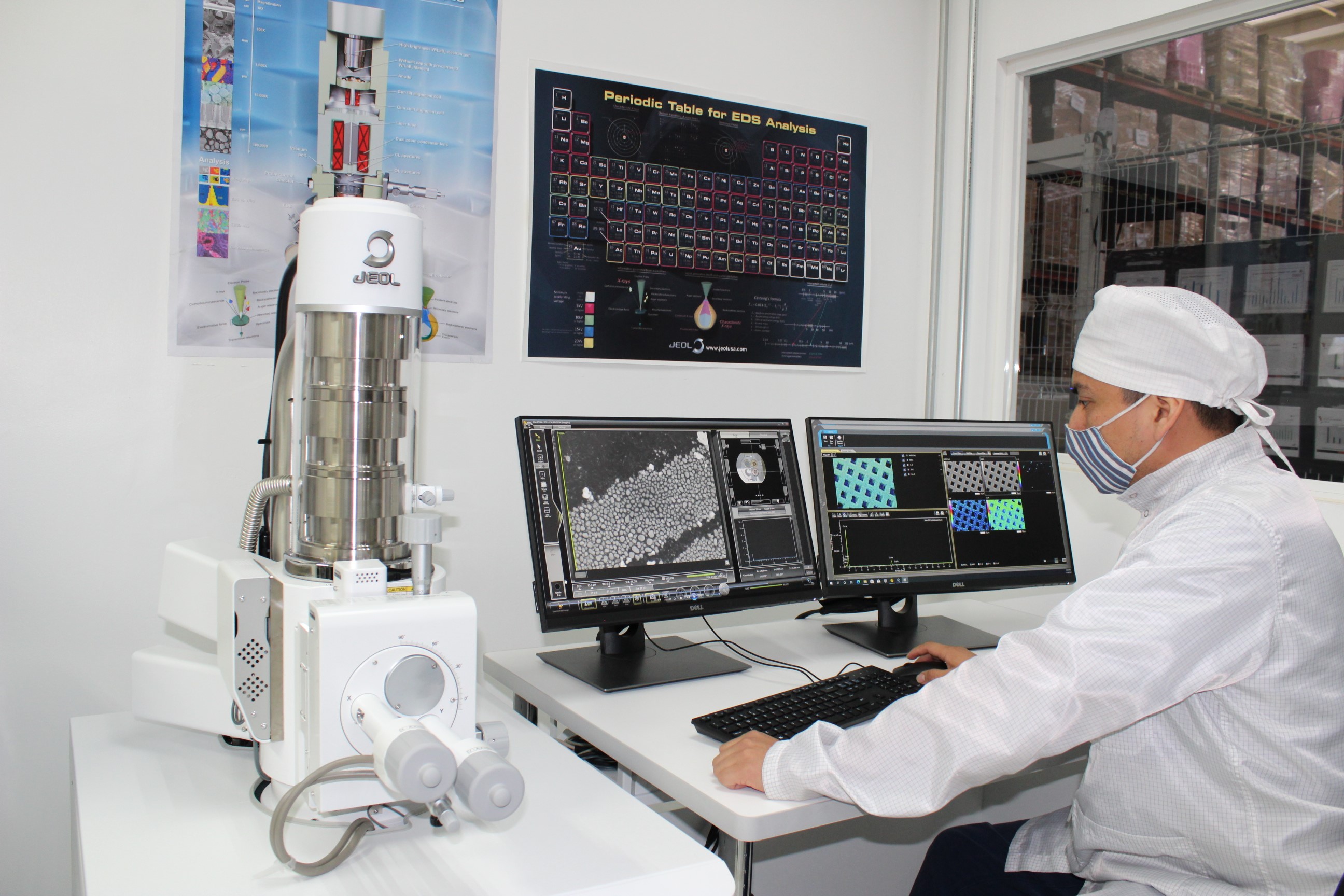
SEM/EDX: Providing powerful microscopy analysis
SEM stands for scanning electron microscopy or scanning electron microscope, while EDX stands for Energy Dispersive X-Ray Analysis (EDX).
SEM produces images that contain information about the surface topography and composition of a sample, while EDX is a technique that enables the elemental analysis of materials.
In SEM, a focused electron beam scans the surface of a sample. This interaction between the beam and the sample generates backscattered electrons, secondary electrons, and X-rays, which are captured to create a magnified image.
The SEM uses the backscattered electrons (BSE) and secondary electrons (SE) for imaging. BSEs come from deeper regions of the sample, producing images with contrast. SEs, meanwhile, originate from the surface and provide more detailed topographic information.
The X-rays generated by the electron beam are used by the EDX to identify the elements that are present in a sample. EDX provides both qualitative and quantitative elemental composition, as well as the relative concentrations of each element in the sample.
“Compared to light microscopes, electron microscopes capture images with a much higher resolution,” shares Martin Palacios from JEOL Mexico, an IMI vendor.
“At IMI’s Analytical Testing and Calibration (ATC) laboratory, our SEM/EDX Analysis machine can achieve pin-sharp images at hundreds of thousands of magnifications. It also enables resolution limits down to 3nm point to point.”
Comprehensive analysis for crucial business decisions
SEM/EDX is a vital tool in failure analysis, research and development, and quality control. It is commonly used to analyze die or package cracks and fracture surfaces, bond failures, and physical defects on the die or package surfaces. It is useful for detecting, isolating, and identifying contamination, investigating delamination, evaluating thin coating, and analyzing integrated circuit failure.
“As opposed to sending samples to an external laboratory, our ATC lab delivers faster results to our customers,” Juan Vázquez, Senior Reliability and Failure Analysis Technician explains. “From whisker and solderability inspection to particle analysis, we can detect welding faults and potential contamination of PCBAs in real time.”
“We help companies pinpoint defects, analyze failures, and select appropriate materials–all of which can optimize their production process. By providing our customers with highly reliable and comprehensive analysis results, they can make critical business decisions and get a safe, durable quality product to market quickly and economically,” says Vázquez.
(Also read: The Importance of Testing Materials)
Your innovative partner for customized solutions
For more than forty years, excellence, customer focus, integrity, and concern for others have been at the heart of IMI. We are committed to providing manufacturing excellence and expertise in the many markets we serve.
IMI’s Analytical Testing and Calibration (ATC) Laboratory is ISO17025 accredited and equipped to deliver rapid and efficient failure analysis, reliability testing, and calibration services while adhering to strict quality standards.
To learn more about our ATC laboratory, download our brochure.
As one of the Top 21 EMS companies in the world, IMI has over 40 years of experience in providing electronics manufacturing and technology solutions.
We are ready to support your business on a global scale.
Our proven technical expertise, worldwide reach, and vast experience in high-growth and emerging markets make us the ideal global manufacturing solutions partner.
Let's work together to build our future today.
Other Blog