40% Output Boost: IMI Reinvents PCBA Testing

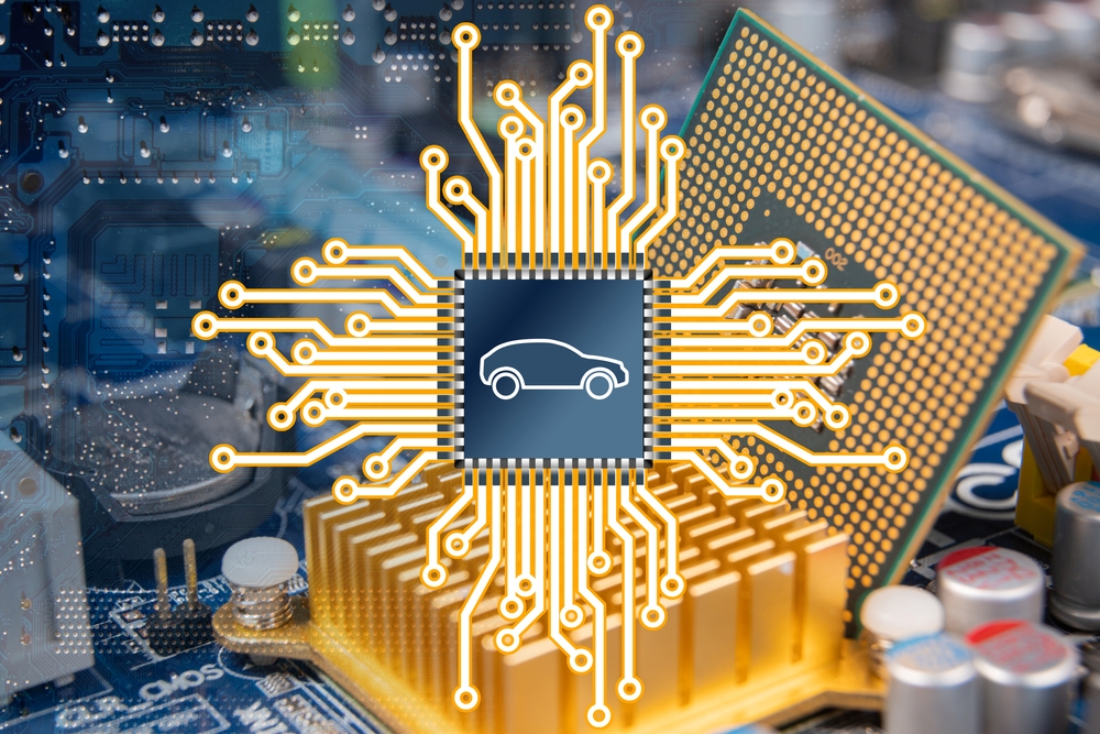
As the global automotive market accelerates toward electrification, electric vehicle (EV) inverters are powering a parallel boom. Stratview Research projects the EV inverter market to surge from $17 billion in 2024 to $40.4 billion by 2031, driven by a 12.4% CAGR. Riding this wave, IMI Jiaxing enabled an EV startup to break into the sector by engineering ultra-dense Printed Circuit Board Assembly (PCBA) modules with high-current inverter circuits—key components for next-gen electric drivetrains.
Ultra‑dense PCBA modules featuring high‑current inverter circuitry are a game‑changer for EVs, combining compactness with power output, economic value, and reliability. These modules pack tightly integrated power semiconductors, often wide bandgap devices like Silicon Carbide (SiC) or Gallium Nitride (GaN), in a minimal form factor. This improves power density and reduces overall inverter size and weight.
Because these high‑current inverters must switch large currents rapidly, heat generation is a major concern. Ultra‑dense designs require advanced thermal management techniques, such as direct double‑sided cooling, thermal vias, metallic ribbon bonding, or liquid cooling, to maintain reliability and longevity in demanding conditions.
These systems are often validated through rigorous thermal cycling tests and thermal shock tests to ensure durability under fluctuating temperatures. Proper design also helps make the electrical signals cleaner and faster by reducing unwanted resistance and interference, which keeps the system running smoothly and efficiently.
(Also read: Top Trends in the Power Electronics Market)
Why ultra-dense PCBA matters for EVs
Ultra-dense power module assembly is reshaping how EVs manage energy, offering a smarter, more compact approach to high-current inverter design. Here are its benefits.
- Exceptional power density
Embedding power devices into the PCB and using thicker copper layers allows ultra-dense PCBAs to deliver more power in a much smaller space, while also enhancing heat handling and reliability. By combining these features with surface mount technologies, this technique significantly boosts power density and reduces electrical interference.
- Cleaner signals & faster switching
Embedding semiconductors directly into the PCB using tiny connection holes (micro vias) removes the need for extra wiring and helps electricity flow more smoothly. This allows GaN or SiC devices to switch faster.
- Weight & size reduction
Compact ultra-dense PCBAs can reduce system weight by tens of kilograms per vehicle. Vicor reports up to 25 kg weight savings in power modules alone. Smaller, lighter inverter modules contribute directly to greater EV range and better packaging flexibility.
- Integration & cost benefits
Multi-layer, high-density interconnect (HDI) layouts with embedded components reduce wiring, simplify assembly, and cut material costs. Optimized copper paths also lower energy loss and heat, boosting efficiency and the system’s overall economic value.
(Also read: Managing the Cooldown for EVs)
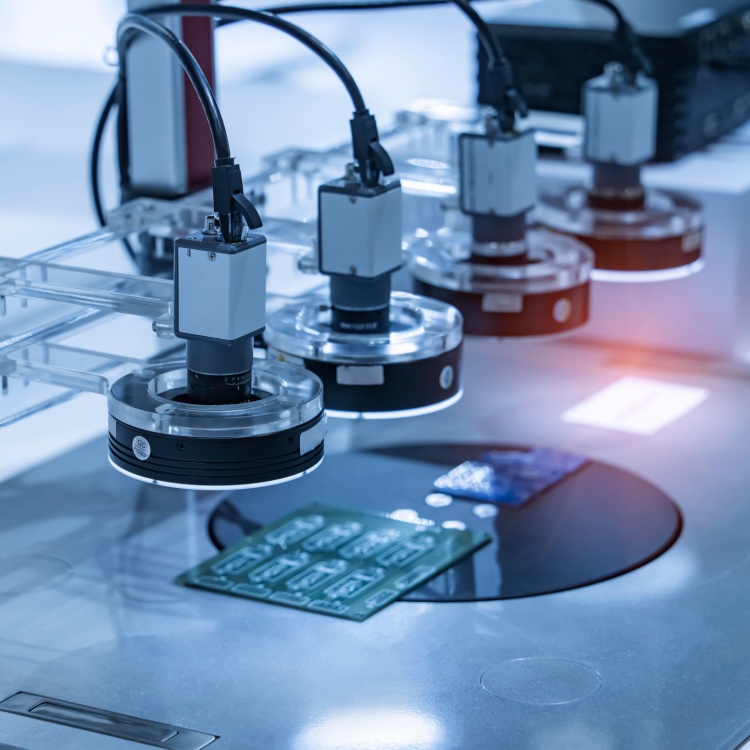
IMI Jiaxing reinvents EV PCBA testing
When a tier-1 client faced mounting challenges with testing ultra-dense PCBA modules for high-current inverter circuits, they turned to IMI Jiaxing for a more refined solution. Traditional spring-pin fixtures posed risks, damaging delicate traces or requiring long downtimes just to switch between board variants. The stakes were high: these next-generation power assemblies demanded accuracy, care, and speed.
IMI Jiaxing’s engineering capabilities were put to the test when the team developed a custom vacuum-clamp test fixture tailored to the client’s needs. The design relied on the principle of differential air pressure, using a sealed chamber between the fixture and the board to create a vacuum that gently yet firmly held the PCBA in place. By removing the need for mechanical clamps, the fixture minimized the risk of damaging dense circuit layouts while ensuring stable and accurate measurements.
The vacuum fixture was engineered with precision. Soft gaskets made from low-durometer silicones or urethanes cushioned the board without leaving marks. Contact surfaces featured ESD-safe, non-marring materials like PEEK and Delrin to prevent static buildup and mechanical abrasion. Recessed cavities in the fixture allowed sensitive components to sit safely below the clamping plane, avoiding unwanted pressure.
To ensure uniform support, the fixture used adjustable, low-profile pins with soft tips that evenly distributed the vacuum's hold-down force across the board. Gaskets were strategically positioned to seal only around non-critical areas such as PCB edges or designated keep-out zones, while avoiding delicate circuits. Each material and design element was chosen with a focus on reliability and board safety.
Positioning accuracy was also a top priority. The fixture featured precision locating pins to engage tooling holes, edge stops for alignment, and optional transparent sections for visual verification before the vacuum locked in. This thoughtful design streamlined the setup process and enabled quick transitions between board variants, significantly reducing downtime.
(Also read: How 3D Printing Breaks Manufacturing Rules in the Best Way)
High-power testing
To test high-current inverters safely and accurately, IMI Jiaxing developed and built a fully automated test system using LabVIEW software. The system, designed from the ground up, loads a pre-set configuration file that defines what to check, which values to measure, and how to determine if a unit passes or fails.
Managing heat during product testing was a key concern. The system used infrared cameras to monitor temperatures in real time. If the heat rises more than 15°C during a 100-amp test, heavy-duty fans automatically switch on. For even more demanding 400-amp tests, special liquid-cooled connectors kept the equipment from overheating.
Safety measures were put in place at every level. The setup includes physical barriers to contain any arc flashes and ultra-fast fuses that shut down power in under 2 microseconds. It also used sensors that spot sudden current spikes and infrared cameras that stopped tests if any area gets hotter than 85°C, helping prevent damage before it starts.
To handle fast electrical spikes during reliability testing, the team used special sensors that reacted in under 5 microseconds and could track changes up to 30 million times per second. They also kept electrical noise from interfering by running tests inside shielded rooms and using high-precision probes.
To make sure readings stayed accurate, they used ultra-precise power meters and special wiring that reduced errors. For product validation, the system had two separate power sources that could switch instantly if one failed, along with ground-fault detectors that caught even tiny issues.
With this advancement, IMI Jiaxing reinforces its role in accelerating the transition to electric mobility. By combining deep engineering expertise with agile test and system development, the team not only solved a complex production bottleneck but also helped a next-gen EV player scale confidently. As the automotive market continues to electrify, IMI’s solutions stand ready to support innovation at the heart of every inverter, module, and mile.

As one of the Top 20 EMS companies in the world, IMI has over 40 years of experience in providing electronics manufacturing and technology solutions.
We are ready to support your business on a global scale.
Our proven technical expertise, worldwide reach, and vast experience in high-growth and emerging markets make us the ideal global manufacturing solutions partner.
Let's work together to build our future today.
Other Blog