Top Trends Shaping Silicon Wafers Today
The silicon wafer sector is entering a new and bold phase as the semiconductor industry evolves to meet the demands of the next generation. With artificial intelligence (AI), smart mobility, and advanced computing raising the bar, wafer technology is being reimagined to stay future-ready. As global demand intensifies and innovation speeds up, 2025 stands out as a turning point for industrial manufacturing.
After a period of sluggish activity, the silicon wafer market is showing signs of a turnaround. According to SEMI, wafer shipments are expected to grow by 10% in 2025, driven by renewed demand from sectors like AI and advanced packaging. This follows a slight decline in 2024 and suggests a recovery is already taking shape.
While demand from the automotive and industrial markets remains subdued, applications tied to AI and high-performance computing are helping stabilize the market. Recent quarterly growth in wafer shipments supports this trend, showing growing momentum despite lingering uncertainty in some sectors.
New investments also point to long-term confidence. Companies are building out production capacity, and government incentives, particularly in the US and EU, are encouraging domestic manufacturing. This marks a shift toward strengthening supply chain management and preparing for future growth.
The silicon wafer market is gradually shaking off its stagnation and beginning to show signs of renewed movement. As inventories normalize and end-use demand picks up, the outlook for silicon wafers is beginning to improve, with signs of sustainable growth on the horizon.
(Also read: What Happens to the CHIPS Act Now?)
10 trends shaping wafer technology
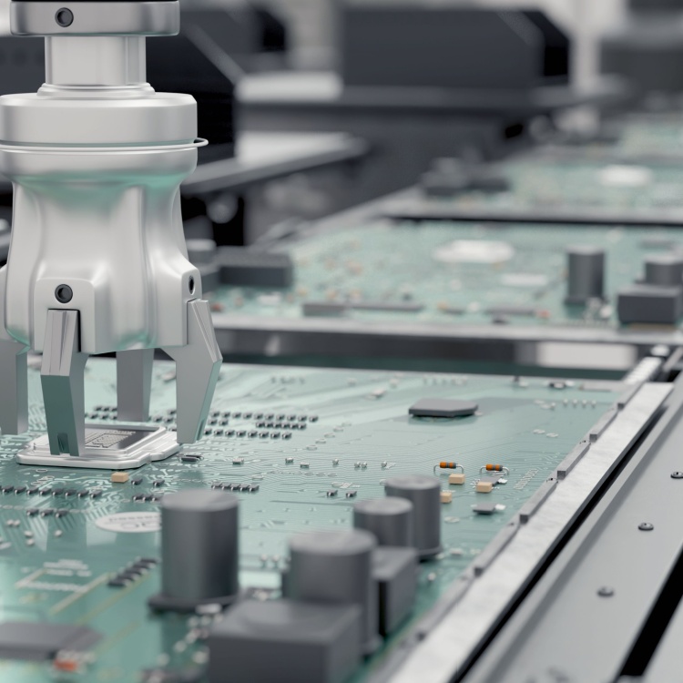
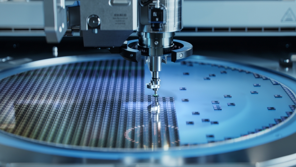
As manufacturing markets evolve, silicon wafer technology is advancing to meet the growing demands of next-generation devices and applications.
- Strengthened wafers at the nanoscale
Swedish startup EPINOVATECH is enhancing the economic value of modern chips with its NovaGaN process, which reinforces silicon wafers at the nanoscale and coats them with gallium nitride (GaN). This innovation boosts performance and operational efficiency, enabling faster, cooler, and smaller transistor devices that lower power use.
- Miniaturization
As 2-nanometer chips enter mass production, the semiconductor industry marks a leap in miniaturization and efficiency. These ultra-compact nodes boost processing speed, cut power use, and generate less heat—unlocking better performance for mobile devices, AI systems, and high-performance computing, while paving the way for more powerful, energy-smart technologies.
- Advanced node technologies
As chipmakers move toward 2-nanometer and 1.8-nanometer production by 2025, fabs face growing pressure to adopt advanced lithography and materials. These next-level nodes push silicon processing to new extremes, making reliability testing more critical than ever. The challenge is scaling down without sacrificing stability, yield, or long-term performance.
- Packaging precision machinery
China-based startup TSD Semiconductor builds advanced machinery designed for modern chip packaging processes. Its tools support wafer thinning, cleaning, and polishing, which are critical steps in modern chip packaging. Used in flip chip assembly and system-in-package builds, the equipment supports manufacturing solutions and meets the demands of high-efficiency designs.
- Progress in EUV and High-NA tech
High Numerical Aperture (High-NA) systems are advancing Extreme Ultraviolet (EUV) lithography, marking a key step forward in precision chipmaking. Promising sharper resolution and tighter transistor packing, these systems can transform chipmaking and influence product design and development. Their complexity, however, demands new materials across fabrication workflows.
- New manufacturing capabilities
As chips shrink to nanoscale dimensions, design and engineering challenges grow more complex—from pattern precision to managing metal-induced wiring delays. In response, startups are reimagining semiconductor production using robotics and additive manufacturing. These innovations streamline fabrication, enabling faster, more cost-efficient chipmaking with greater accuracy.
- 3D chip stacking and mixed packaging
Heterogeneous integration and 3D chip stacking are poised to reshape electronic manufacturing in 2025. Innovations like wafer bonding, advanced interconnects, and through-silicon vias enable vertical assembly of logic, memory, and I/O components. This compact packaging approach boosts performance and shrinks device size.
- Chemical defect inspection
Swiss startup UNISERS offers an analytical testing solution that helps chipmakers detect nanoscale chemical defects during semiconductor production. By combining precision coatings, optical inspection, and smart data analysis, the system identifies particle size, composition, and distribution. This minimizes contamination risks and improves reliability in high-purity processes.
- Chip tracking systems
Canada’s Digitho is tackling chip traceability challenges with a die-level ID system powered by digital lithography. By marking chips early in the wafer process, the startup enables full lifecycle tracking across fragmented supply chains. Its verification tools also support recycling efforts, reducing reliance on raw materials.
- AI-centric processors
AI is transforming chip design, driving smarter, faster processors that handle complex tasks in real time. Neuromorphic chips mimic brain function for efficient learning, while AI-accelerated hardware powers edge computing. These innovations are expanding applications in smart mobility, robotics, and urban infrastructure with greater speed and adaptability.
- Chiplet-based design
Semiconductor makers are moving away from single-die designs in favor of modular chiplet strategies. By linking smaller, specialized components, they gain flexibility, lower costs, and improved performance. This scalable approach supports faster, more efficient systems across AI, cloud computing, and gaming while adapting to diverse and evolving workloads.
- Designing for efficiency
Chinese chipmakers are rewriting the rulebook on memory speed. Researchers at Shanghai’s Fudan University unveiled PoX, a groundbreaking non-volatile memory device that writes data in just 400 picoseconds, which is far faster than traditional flash memory. By merging ultra-fast write speeds with data retention, PoX promises major gains in energy-efficient AI computing.
- Recovered silicon carbide (SiC)
Hard Blue Si-Carbons, a U.S. startup, turns agricultural waste into high-value SiC for semiconductor use. Instead of traditional fuel conversion, it recovers abrasive-grade materials from farm residues. This process reduces the need for mined inputs, cutting both costs and emissions for chipmakers using SiC in wafers and tooling.
- Next-gen power semiconductors
SiC and GaN are transforming power electronics in response to growing demand for sustainability and speed. Known for their fast-switching capabilities and resilience to heat, these wide bandgap semiconductors are key to improving energy use across modern technologies. They're now critical to powering electric vehicle (EV) infrastructure, telecom systems, and industrial tech with greater speed and reliability.
- Energy-smart sustainability
The combination of escalating energy costs and environmental concerns is driving chip producers to implement more sustainable manufacturing practices. Techniques such as chemical reuse, water recovery, and low-energy etching are gaining ground. Companies embracing sustainable fabrication stand to gain regulatory support and market advantages as environmental responsibility becomes central to industry competitiveness.
(Also read: Flip Chip Tech Is Here to Stay)
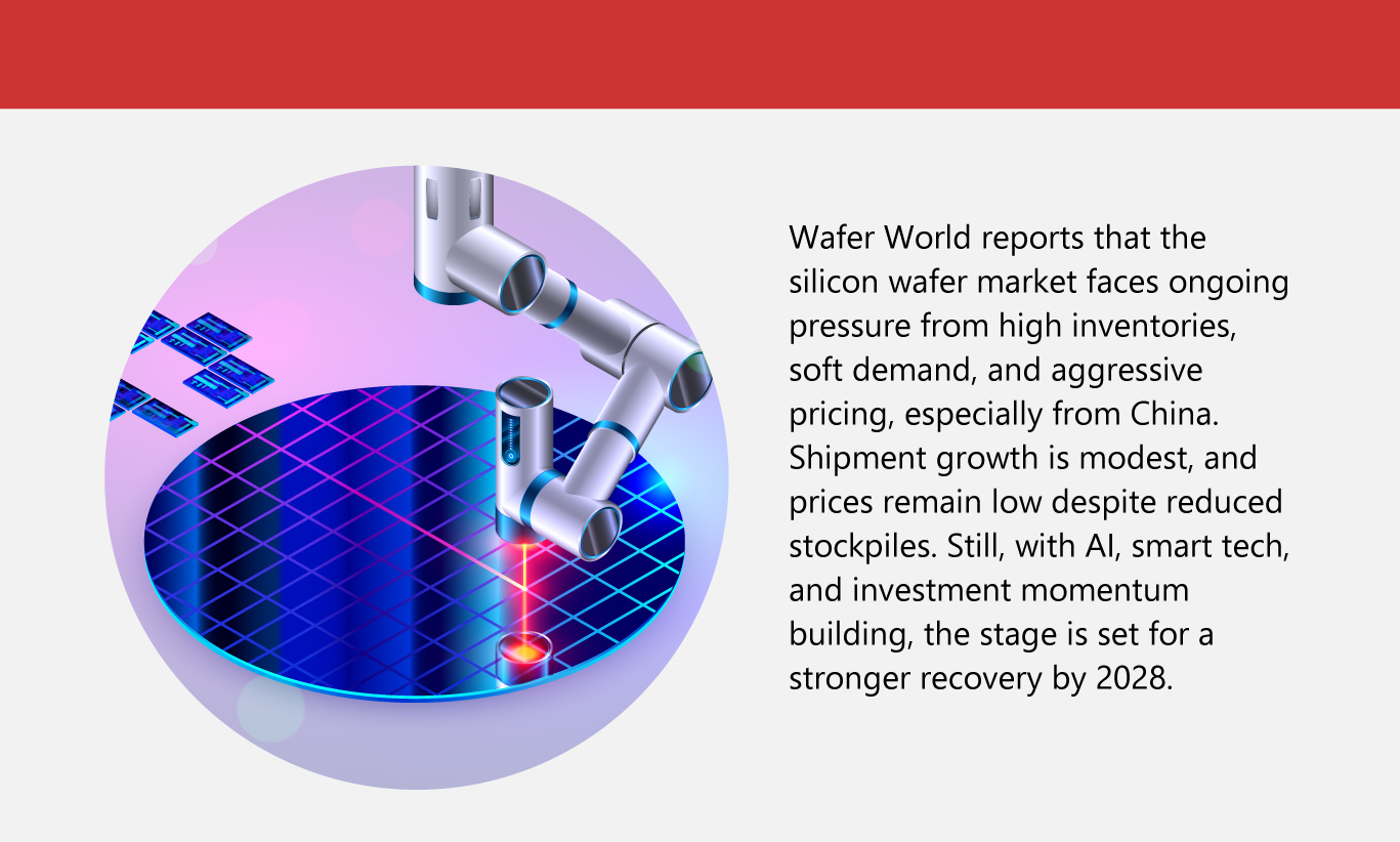
Wafer World reports that the silicon wafer market faces ongoing pressure from high inventories, soft demand, and aggressive pricing, especially from China. Shipment growth is modest, and prices remain low despite reduced stockpiles. Still, with AI, smart tech, and investment momentum building, the stage is set for a stronger recovery by 2028.
As silicon wafer innovation gains momentum, the industry is showing signs of renewed resilience. With smarter materials, sustainable practices, and strategic investment shaping the landscape, chipmakers are better equipped to navigate ongoing challenges. These shifts point to a more stable and forward-looking path for semiconductor manufacturing.

As one of the Top 20 EMS companies in the world, IMI has over 40 years of experience in providing electronics manufacturing and technology solutions.
We are ready to support your business on a global scale.
Our proven technical expertise, worldwide reach, and vast experience in high-growth and emerging markets make us the ideal global manufacturing solutions partner.
Let's work together to build our future today.
Other Blog