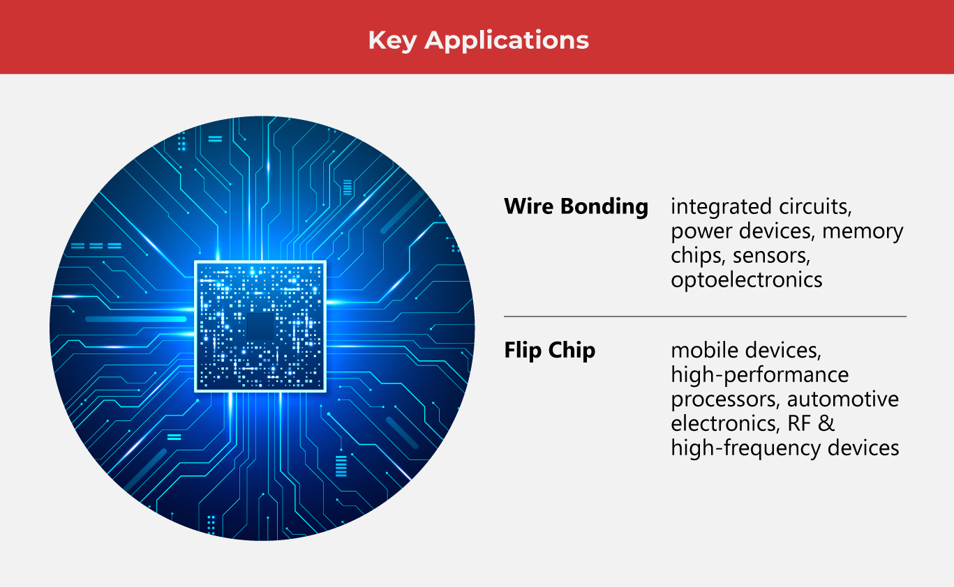
Wire Bonding vs. Flip Chip: Which Wins?
Interconnect technology in electronics manufacturing has progressed from simple wire-based links to advanced integration methods that enable today’s high-performance devices. Among the most widely used approaches, wire bonding and flip-chip bumping dominate as key techniques for attaching semiconductor dies to their packages.
Wire bonding, introduced in the 1950s, has long been used to connect semiconductor dies to package substrates. It has evolved through gold, aluminum, and copper materials, improving cost, reliability, and electrical performance.
Meanwhile, flip-chip technology emerged in the 1960s as an alternative, developed by IBM under the Controlled Collapse Chip Connection (C4) process. Unlike wire bonding, it uses the full die surface for interconnections, enabling higher input/output (I/O) density and shorter electrical paths for improved performance in advanced surface mount technology systems.
Ongoing demand for device miniaturization has pushed steady innovation in semiconductor interconnect technologies. While the global wire bonding market remains stable at around $5 billion annually, supported by case uses in the analog, IoT, and automotive markets, faster growth is being seen in advanced alternatives. Flip-chip technology, in particular, is expanding rapidly and is projected to surpass $40 billion by 2030.
To determine the most suitable interconnect technology for your specific needs, we examine each option and evaluate its strengths and limitations.
Wire Bonding: A Closer Look
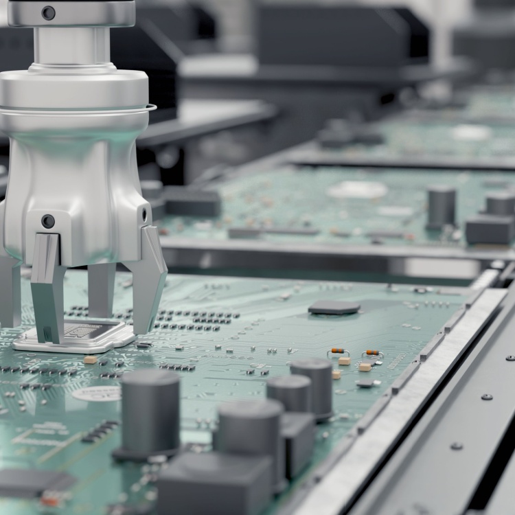
Wire bonding is a well-established interconnection technique widely used across the semiconductor industry and continues to serve as a reliable industrial solution for connecting integrated circuits to their packages or substrates. It uses fine metallic wires, typically copper, gold, and aluminum, to form electrical connections between chip terminals and package leads or printed circuit boards (PCB). The process relies on thermal, ultrasonic, or combined energy to create strong and stable bonds, making it a proven method that delivers consistent economic value.
There are two primary bonding approaches used in wire bonding. Ball bonding, often associated with gold wire, begins by forming a small molten ball at the end of the wire, which is attached to the bond pad using heat and pressure. The wire is then routed to the second bond point, where it is secured using ultrasonic energy. In contrast, wedge bonding typically uses aluminum wire and does not require ball formation; instead, the wire is directly pressed onto the bond pad, often at room temperature, making it suitable for specific thermal-sensitive applications.
The wire bonding process involves substrate cleaning and preparation, precise placement of the semiconductor die, careful wire positioning, bonding at designated pads, trimming excess wire length, and optional encapsulation to enhance protection and reliability. This structured process is supported by mature equipment and well-established production workflows.
Despite its advantages, wire bonding has inherent limitations. It offers lower I/O density compared to more advanced interconnect methods, requires longer interconnect paths that can affect electrical performance, and often leads to larger chip footprints due to peripheral pad layouts. It is also less suited for high-frequency applications where parasitic effects such as capacitance and inductance can degrade performance.
Deep Dive into Flip Chip Technology
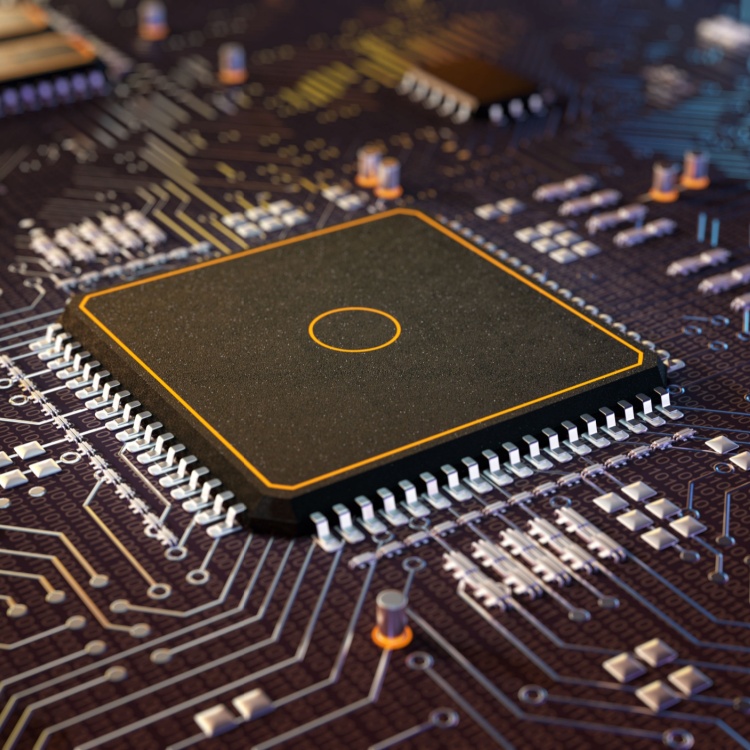
Flip chip is an advanced semiconductor packaging approach in which the die is flipped and attached directly to the substrate using microscopic solder bumps. This configuration replaces traditional wire-based connections with direct face-down interconnection, allowing the active surface of the chip to interface closely with the package in a highly compact structure used across modern electronics systems.
The architecture enables shorter electrical paths, higher input/output density, and improved overall signal performance. In thermal analysis, flip chip packages are often highlighted for their efficient heat transfer capability due to direct die-to-substrate contact and the possible addition of heat spreaders.
The manufacturing flow includes wafer bumping, precision dicing, die alignment, reflow soldering or thermal compression bonding, and underfill dispensing. The underfill material is critical, as it distributes mechanical stress and helps compensate for differences in thermal expansion between silicon dies and organic substrates, improving structural durability during operation.
Despite its benefits, flip chip technology introduces greater process complexity and higher production cost compared to wire bonding. It demands micron-level placement accuracy, advanced inspection methods such as X-ray analysis, and strict process control during reflow and underfill stages. Challenges such as void formation, thermal expansion mismatch, and solder joint fatigue remain key concerns, particularly under extended thermal cycling test conditions in high-performance and mission-critical applications.
(Also read: Top 7 Advantages of Using Chip on Board Tech)
Interconnect Technology Comparison: Flip Chip and Wire Bonding in Practice
From an electrical performance standpoint, flip chip offers a clear edge because its interconnects are extremely short, reducing parasitic resistance, capacitance, and inductance. This supports faster signal transfer and improved operational efficiency in high-speed designs. Wire bonding, while less electrically optimal, can still deliver solid performance when supported by engineering capabilities, including optimized pad layout, careful selection of wire diameter, prioritization of key signal paths, and improved substrate routing.
In thermal behavior, flip chip generally performs better due to direct die-to-substrate contact, which improves heat dissipation. Wire-bonded packages can still be strengthened through thermal design strategies such as added copper thickness, higher via density, thermal via arrays, multi-layer substrates, and the use of heat spreaders or metal slugs to improve heat flow and stability.
For size and integration density, flip chip enables compact architectures with high I/O capability since connections span the full die surface. Wire bonding requires perimeter bonding areas and looped wires, resulting in a larger footprint, although staggered pad layouts can help improve density in certain designs.
On cost and manufacturability, wire bonding remains more economical for lower complexity and lower volume production due to its mature and flexible process flow. Flip chip becomes a more cost-efficient manufacturing solution at higher scales and advanced applications, but requires tighter alignment control, more complex assembly steps, and stricter process conditions.
After reliability testing, both approaches are viable when properly designed. Wire bonding has a long track record across industries, while flip chip delivers strong performance in demanding environments, especially when paired with underfill materials that reduce stress from thermal expansion mismatch and improve long-term mechanical durability.
Future-Ready Interconnect Technologies: What’s Ahead
Wire bonding and flip chip technologies are both advancing to meet growing demands for smaller, faster, and more efficient electronic devices.
Wire bonding is evolving through finer pitch capabilities, the use of alternative materials like copper for better cost and performance, and improved process control for higher yield and reliability.
Meanwhile, flip chip development is focused on further reducing bump sizes to increase input/output density, enhancing underfill materials for greater mechanical stability, and enabling integration with advanced 2.5D and 3D packaging solutions.
Overall, both interconnect methods are expected to coexist, with selection depending on performance needs, design constraints, production scale, and cost efficiencies.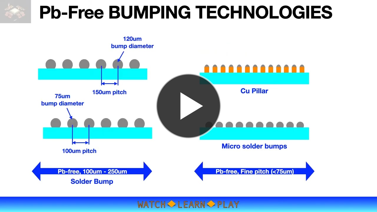 As one of the Top 30 EMS companies in the world, IMI has over 40 years of experience in providing electronics manufacturing and technology solutions.
We are ready to support your business on a global scale.
Our proven technical expertise, worldwide reach, and vast experience in high-growth and emerging markets make us the ideal global manufacturing solutions partner.
Let's work together to build our future today.
Other Blog