
The Future of Power SiC and GaN
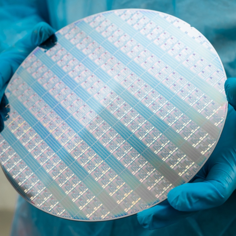
The global shift toward electrification demands high-performance power conversion, placing wide-bandgap materials like SiC and GaN at the center of innovation. While these semiconductors offer unmatched efficiency and power density, their true capabilities are limited by current packaging technology.
As SiC and GaN devices push operational junction temperatures beyond 175°C and reach megahertz-level switching frequencies, the materials responsible for cooling and interconnecting these chips have become the primary performance bottleneck.
In the realm of electronic manufacturing, power module packaging serves as the essential bridge between the bare die and the intense mechanical and thermal rigors of the end application. Components such as ceramic substrates, die attach pastes, and encapsulants account for a fraction of the finished module price, yet they rarely receive the same level of scrutiny as the semiconductor itself.
To ensure these modules survive the transition to higher power levels, packaging materials must pass intensive thermal cycling tests to prevent premature failure. By shifting the focus toward these critical processed components, manufacturers can overcome the current technical limitations and fully realize the reliability and miniaturization benefits.
Forces Fueling the Shift
SiC is rapidly moving from niche technology to a core requirement in modern power electronics. This evolution is dismantling decades of reliance on legacy silicon Insulated-Gate Bipolar Transistors (IGBTs), forcing a total reimagining of the materials that house and protect these high-performance chips.
The primary driver is a relentless pursuit of efficiency and power density within the automotive market, particularly in the EV sector. For instance, a traditional medium-voltage fast charger setup that once required a massive transformer and converter can now be replaced by a SiC-based solid-state system that is a mere fraction of the original weight. This radical reduction in mass is accompanied by a meaningful increase in efficiency, providing a critical performance margin in the competitive EV and renewable energy markets.
However, the superior performance of SiC comes with punishing physical demands, as these modules must maintain dielectric integrity and operational efficiency at extreme operating temperatures. As a result, the industry is seeing a rapid migration away from conventional solder and aluminum wire toward silver sintering and copper clip architectures that significantly slash parasitic inductance. This transition is vital for reliability, especially considering that a standard city charger is expected to endure tens of thousands of thermal cycles over its operational lifespan.
The supply chain for these critical materials remains a complex geopolitical puzzle. While China is aggressively expanding its domestic capacity, Japan continues to dominate the industrial manufacturing of ultra-high-purity copper powders and ceramics. This concentration of power creates significant vulnerability, particularly as silver and copper account for 20 to 22% and 58% of raw material value, respectively, leaving manufacturers exposed to sharp price volatility. Because automotive qualification cycles typically last between two and five years, diversifying these supply chains is a slow, methodical process.
Despite these hurdles, the packaging materials market is projected to see high-single-digit growth through 2036, catalyzed by the fact that SiC Metal-Oxide-Semiconductor Field-Effect Transistors (MOSFETs) are expected to account for more than 30% of all EV traction inverter shipments by 2030.
(Also read: This Small but Powerful Smart Power Module Is Making Waves)
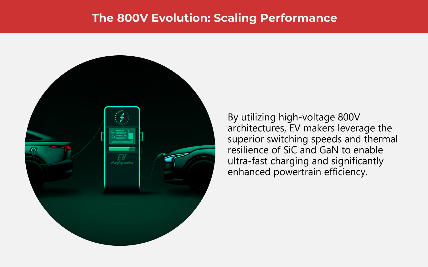
The Shift to 800V Architecture
For years, the EV industry has relied on a standard 400V electrical backbone. However, a transition toward 800V systems is fundamentally changing how EVs are engineered and experienced. The logic behind this shift is rooted in basic physics: by doubling the voltage, engineers can deliver the same amount of power while cutting the electrical current in half. This reduction in current is a game-changer for vehicle design because it significantly lowers the heat generated by resistive losses, allowing for a more efficient and reliable powertrain.
One of the most tangible benefits of moving to a higher voltage is the reduction in vehicle mass. Traditional high-current wiring harnesses are incredibly heavy, often weighing between 60 and 70 kg. Because 800V systems require less current, they can utilize much thinner, lighter copper cables and smaller busbars. Higher voltage allows for slimmer, more flexible charging leads, making the process of plugging in feel less like a workout and more like a seamless chore.
While 800V architecture paves the way for ultra-fast charging, the vehicle’s potential is often dictated by the station it’s plugged into. Modern high-speed charging networks are now deploying hardware that supports up to 1,000V, allowing these advanced vehicles to draw massive amounts of power without overheating the connectors. When a car can accept power at these levels, charging stops become noticeably shorter, making long-distance travel much more practical. However, 400V systems will likely remain the standard for affordable, everyday commuters for the foreseeable future.
Currently, the primary barrier to widespread adoption is the premium price tag associated with high-voltage components. Moving to 800V requires more expensive SiC semiconductors, advanced cooling systems, and specialized insulation. However, as manufacturing technologies and industries scale, these costs will plummet.
Industry analysts project that the price gap for an 800V platform will drop significantly by 2028. As these expenses continue to normalize, the technology will migrate from luxury performance cars into mainstream models, eventually becoming standard across mass-market EV platforms.
(Also read: The Importance of EMS in Boosting EVs)
The Next Frontier
GaN technology has helped power the introduction of advanced bidirectional switches. Unlike traditional configurations that require bulky, back-to-back arrangements, new common-drain architectures allow a single die to manage voltage in both directions. This breakthrough significantly shrinks the hardware footprint while boosting performance.
For example, integrating these advanced switches into solar microinverters can increase power output by 40% without increasing the device size. This shift represents a major leap in engineering capabilities, allowing designers to maximize density while simultaneously driving down total system costs.
Beyond vehicles, GaN is unlocking gains in digital infrastructure. In the high-stakes environment of AI data centers, GaN-based power supplies are slashing energy losses by up to 30%, facilitating more compact and sustainable server architectures. The impact is equally transformative in robotics; motor drives powered by GaN are becoming nearly half the size of their predecessors, providing humanoid robots with the precision required for complex, fine-tuned movements.
As we move through 2026, the superior efficiency and reliability of GaN are positioning it as the primary catalyst for the next generation of energy-efficient global infrastructure.
 As one of the Top 30 EMS companies in the world, IMI has over 40 years of experience in providing electronics manufacturing and technology solutions.
We are ready to support your business on a global scale.
Our proven technical expertise, worldwide reach, and vast experience in high-growth and emerging markets make us the ideal global manufacturing solutions partner.
Let's work together to build our future today.
Other Blog