The Growing Importance of Sic Wafers
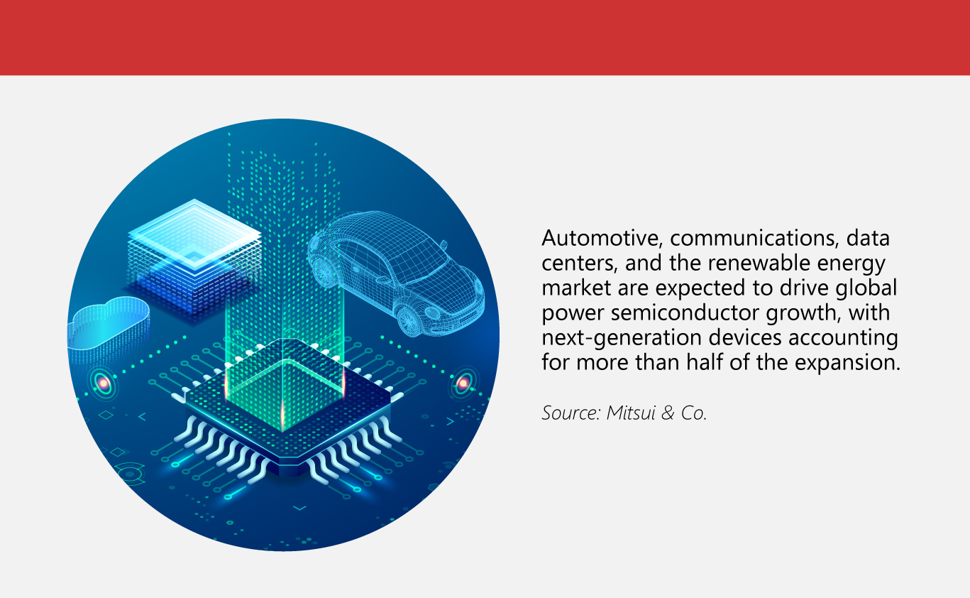
Power semiconductors sit at the core of modern electrical systems, spanning everything from home appliances to infrastructure and increasingly vehicles in the automotive market. The integration of SiC power devices into the hybrid system of Toyota’s next-generation RAV4, the world’s best-selling vehicle in 2024, marked a key milestone and signaled the shift toward broader adoption of advanced semiconductors.
The adoption of SiC power semiconductors in hybrid vehicles, often viewed as a practical bridge for electric mobility that balances environmental indicators with economic value, is gaining momentum in high-volume models. As demand intensifies for smaller, lighter, and more reliable systems, companies across SiC wafer manufacturing, front-end and back-end processes, and module integration are positioned to benefit from this structural growth.
Looking for power module solutions? Explore them here.
SiC Wafers: Pure Power
SiC wafer technology has developed over more than a century, beginning with the Acheson process in 1891 and later gaining attention in the 1950s for semiconductor use. Its appeal stems from inherent material advantages, including a wide bandgap, strong thermal conductivity, high breakdown voltage, and chemical stability, making it well-suited for power electronics and high-temperature environments.
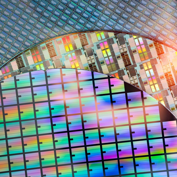
Key advances in crystal growth methods during the 1980s and 1990s enabled higher-quality substrates and larger wafer sizes, paving the way for mass production. By the 2000s and 2010s, wafer scaling from 2-inch to 4-inch and 6-inch formats supported broader adoption, laying the foundation for today’s move toward even larger SiC wafers in high-volume global manufacturing.
Operational efficiency gains from SiC technology are reshaping expectations in power electronics, with devices delivering around 10% better performance than conventional silicon and reducing overall energy losses. This improvement, combined with strong high-temperature capability, supports system miniaturization by enabling smaller, more integrated designs without compromising reliability. As adoption broadens across industries, the global SiC market is forecast to grow at a compound annual rate exceeding 20% through the end of the decade.
(Also read: Top Trends Shaping Silicon Wafers Today)
Advantages of SiC Wafers in Modern Electronics
SiC wafers are built on a crystalline lattice of silicon and carbon, forming a semiconductor material with performance characteristics that extend well beyond traditional silicon. Their intrinsic properties make them particularly suited for demanding power electronics applications where efficiency, durability, and compact design are critical.
One of the most significant advantages of SiC is its ability to operate under extreme conditions. Upon thermal analysis, devices fabricated on SiC wafers can withstand temperatures exceeding 200°C while maintaining stable performance, reducing the need for complex cooling systems.
This high-temperature resilience, combined with strong breakdown voltage capability, allows faster switching speeds and improved energy conversion efficiency. In practical terms,
SiC-based devices can achieve efficiency levels of up to 95%, reducing power losses and improving overall system performance across EVs, renewable energy systems, and industrial power supplies.
As a result, design and engineering teams can create more compact and integrated systems without compromising performance, which is increasingly important in modern electronics where space, weight, and thermal constraints are tightly controlled.
Reliability testing highlights another key strength of SiC technology. The material shows strong resistance to stress-related degradation, making it compatible with mission-critical environments where long service life is essential. For manufacturers and system designers, this results in fewer field failures and more consistent performance under continuous high-load conditions, reinforcing SiC’s role in high-reliability applications.
While traditional silicon continues to dominate cost-sensitive markets due to its mature manufacturing ecosystem, rising demand for higher efficiency and improved thermal performance across industrial markets is steadily positioning SiC as a critical enabling material for next-generation electronics.
(Also read: The Future of Power: SiC and GaN)
Manufacturing and Scaling Challenges
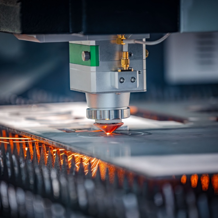
Despite strong momentum in adoption, SiC wafer manufacturing continues to face structural and technical limitations that constrain broader scale-up. One of the most persistent challenges is yield variability in wafer fabrication. Even small defects introduced during crystal growth or processing can significantly affect device performance, making quality control a critical and ongoing requirement rather than a one-time checkpoint. Compared to traditional silicon, SiC still exhibits higher defect densities, which can translate into reduced consistency and increased production costs.
Manufacturers also continue to grapple with the complexity of scaling production to larger wafer sizes. While 4-inch SiC wafers established an early commercial baseline, the industry is steadily transitioning toward 6-inch formats to support higher volumes and lower unit costs. However, this shift is technically demanding, requiring upgrades in equipment, tighter process control, and more advanced crystal growth techniques. As a result, scale-up remains uneven across the supply chain, with only leading producers able to consistently achieve high yields at larger diameters.
Cost remains another key constraint. The production process for SiC wafers is inherently more complex than silicon, involving high-temperature crystal growth and precise defect management. These requirements increase capital intensity and limit the ability of some manufacturing industries to compete at scale. Even established players must continuously invest in process refinement and tool upgrades to maintain competitiveness.
At the same time, the industry operates in a fast-moving environment shaped by rapidly evolving demand. This creates additional pressure on supplier quality while maintaining strict quality standards.
Leading companies continue to push forward, but the broader ecosystem still faces challenges in balancing scale, cost, and reliability. Addressing these constraints will be essential for SiC wafers to fully transition from a high-performance niche material to a mainstream semiconductor platform.
Outlook for SiC Wafer Adoption
Growth in SiC technology continues to follow a clear but challenging trajectory, marked by both strong demand and a necessary learning curve. Companies will need to enhance manufacturing solutions and deepen engineering capabilities to keep up with rapidly shifting technical requirements.
Early-stage applications may not deliver immediate returns, underscoring the need for sustained refinement and innovation. Over time, improvements in SiC wafer development are expected to enable more efficient and reliable energy systems, reinforcing the industry’s ongoing transition toward advanced semiconductor solutions across global markets.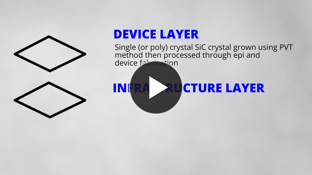 As one of the Top 30 EMS companies in the world, IMI has over 40 years of experience in providing electronics manufacturing and technology solutions.
We are ready to support your business on a global scale.
Our proven technical expertise, worldwide reach, and vast experience in high-growth and emerging markets make us the ideal global manufacturing solutions partner.
Let's work together to build our future today.
Other Blog